0
NLM7000U 7km UAV Tracking Laser Rangefinder Module
NLIR1280ES High-Performance Uncooled Thermal Camera Modules
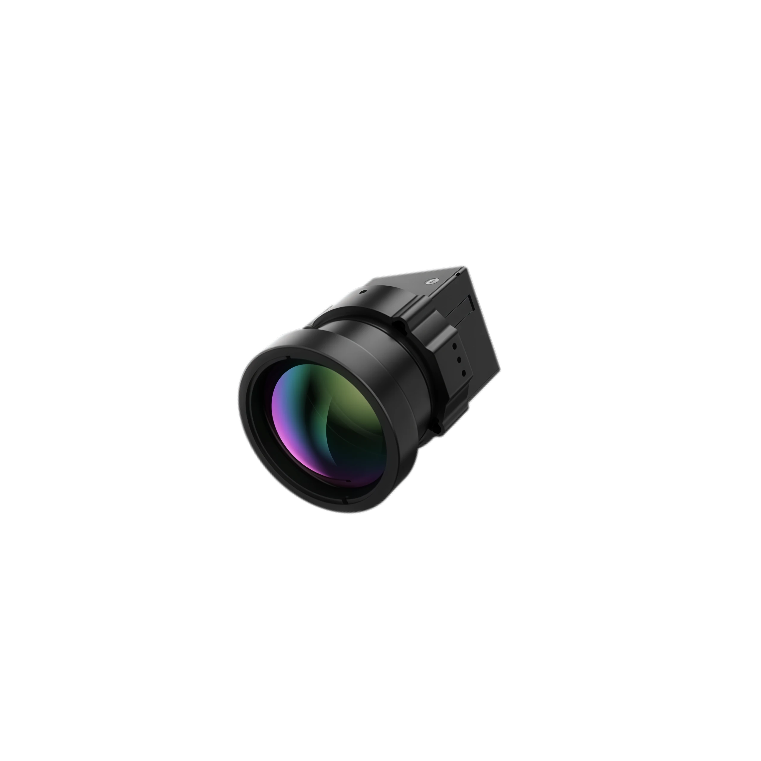
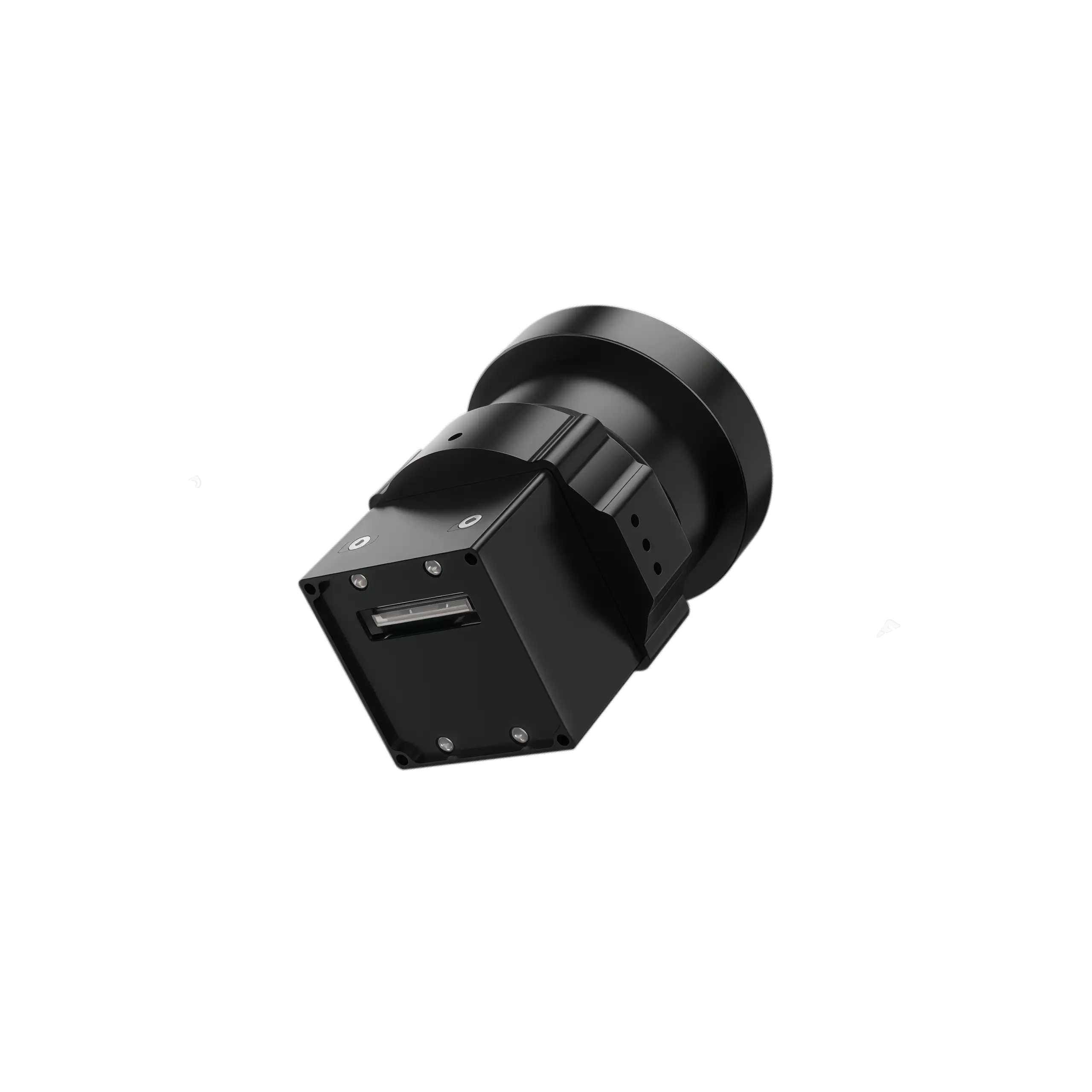
NLIR1280L | Thermal Camera Cores for UAV Payloads
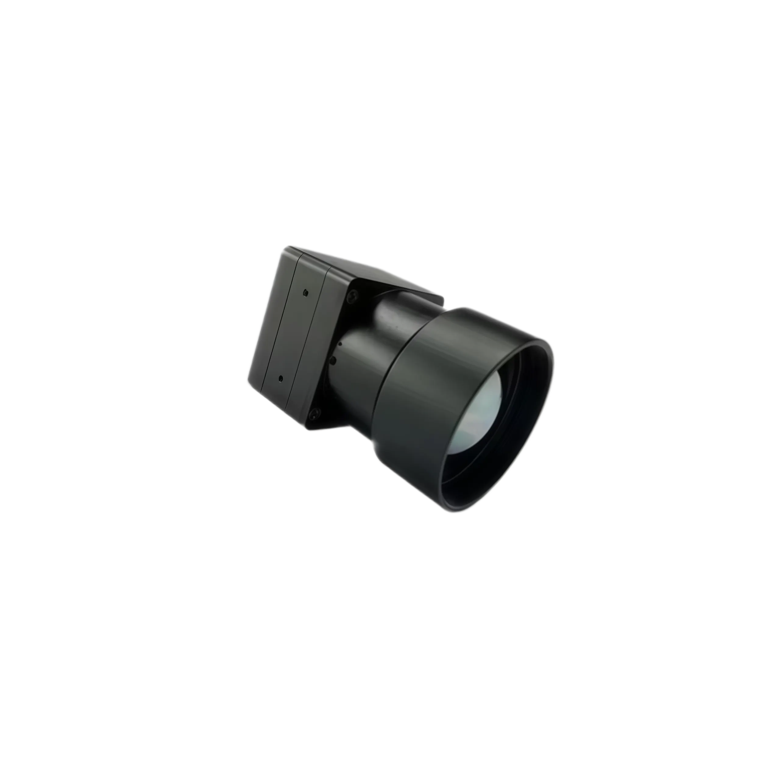
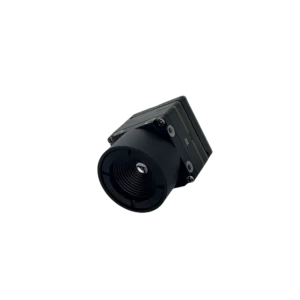
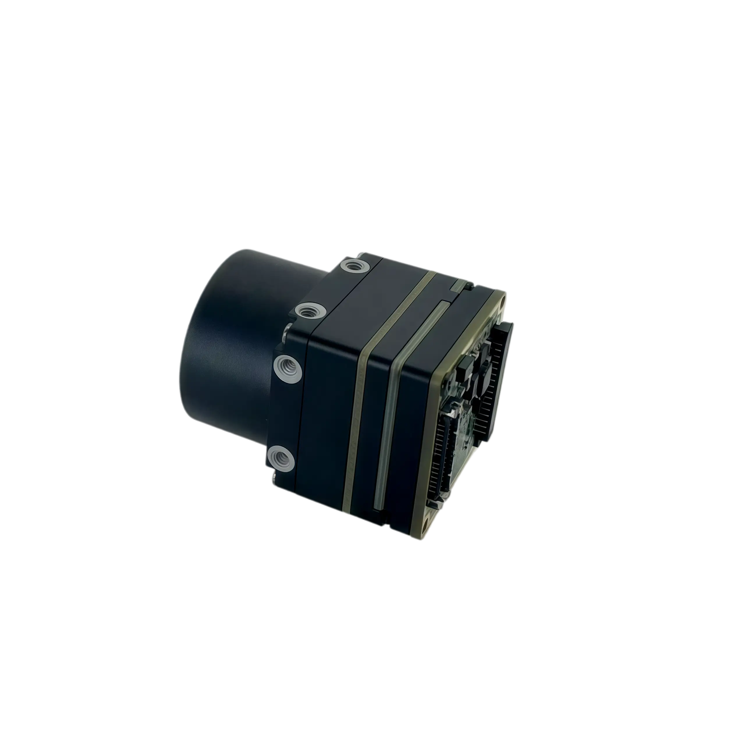
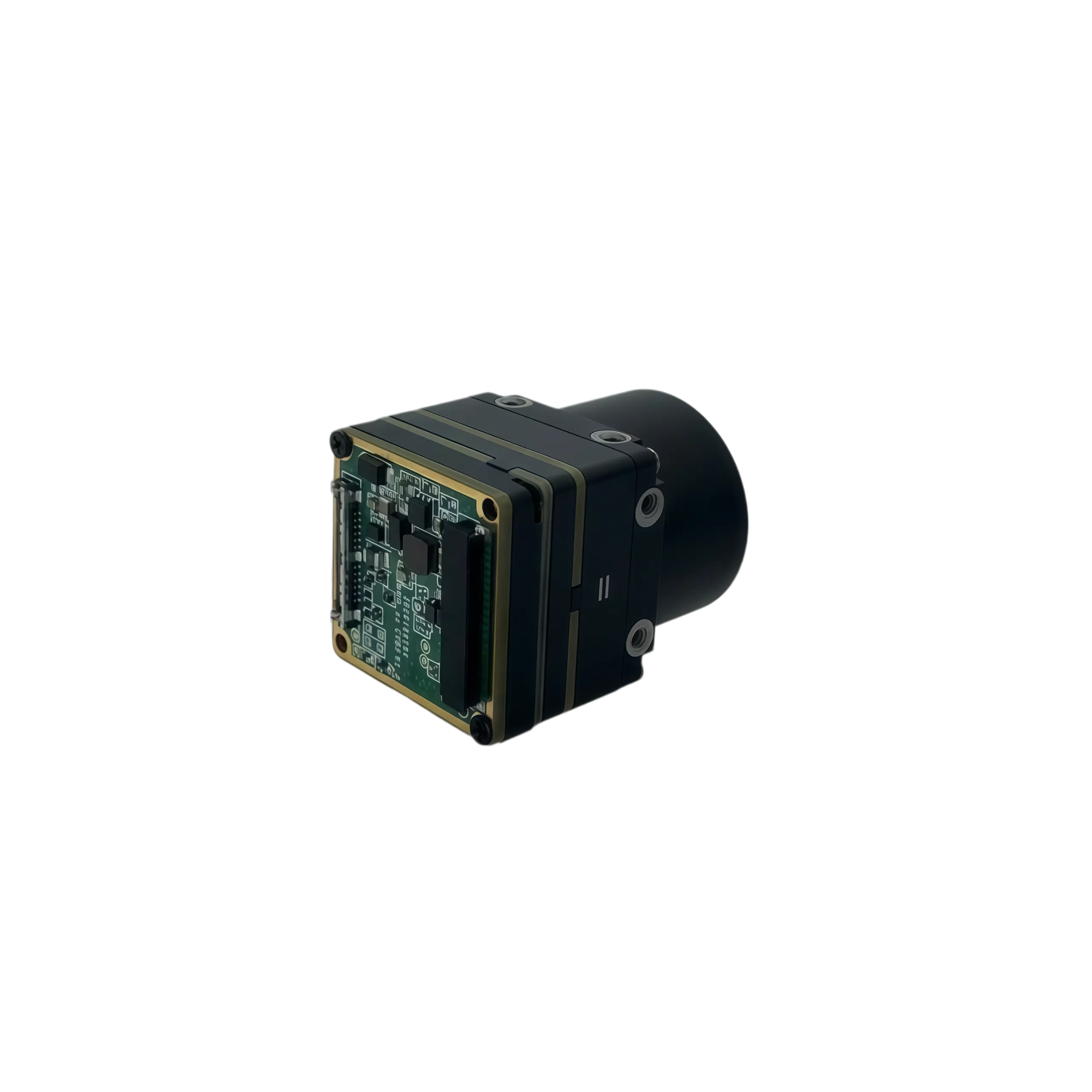
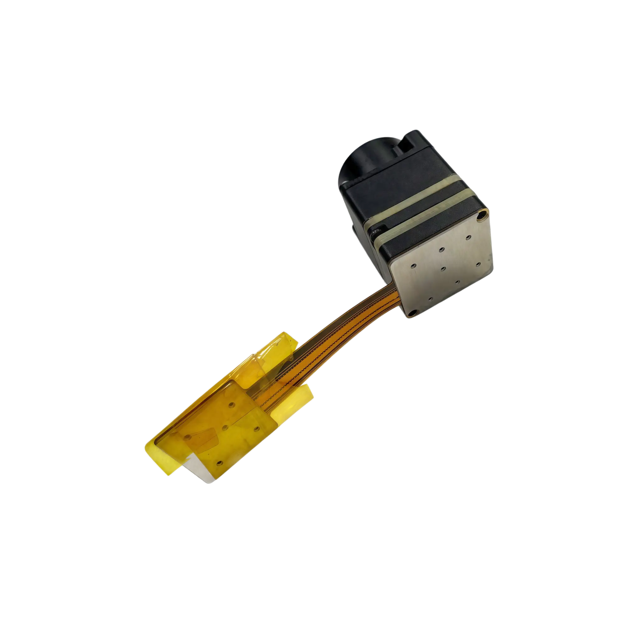
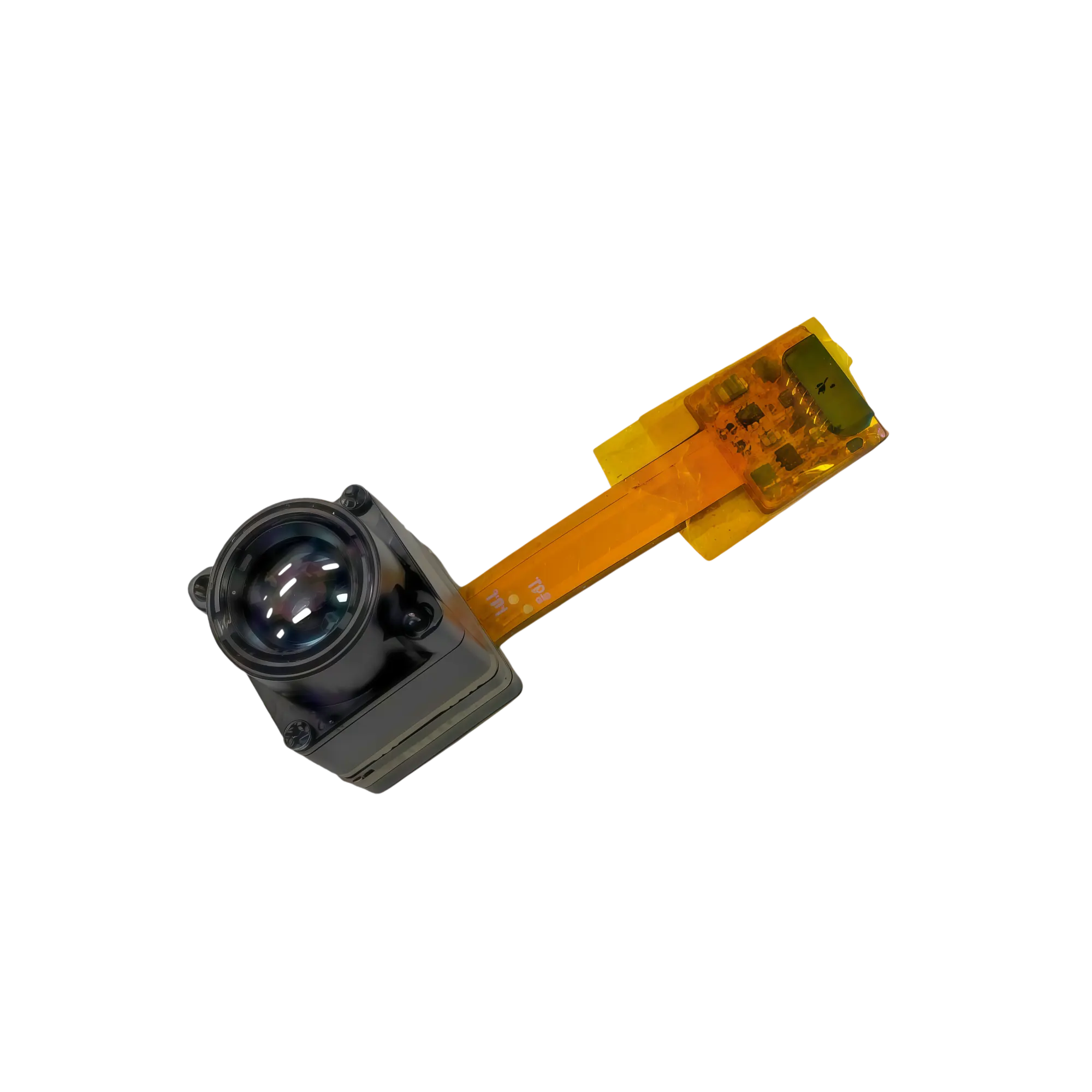
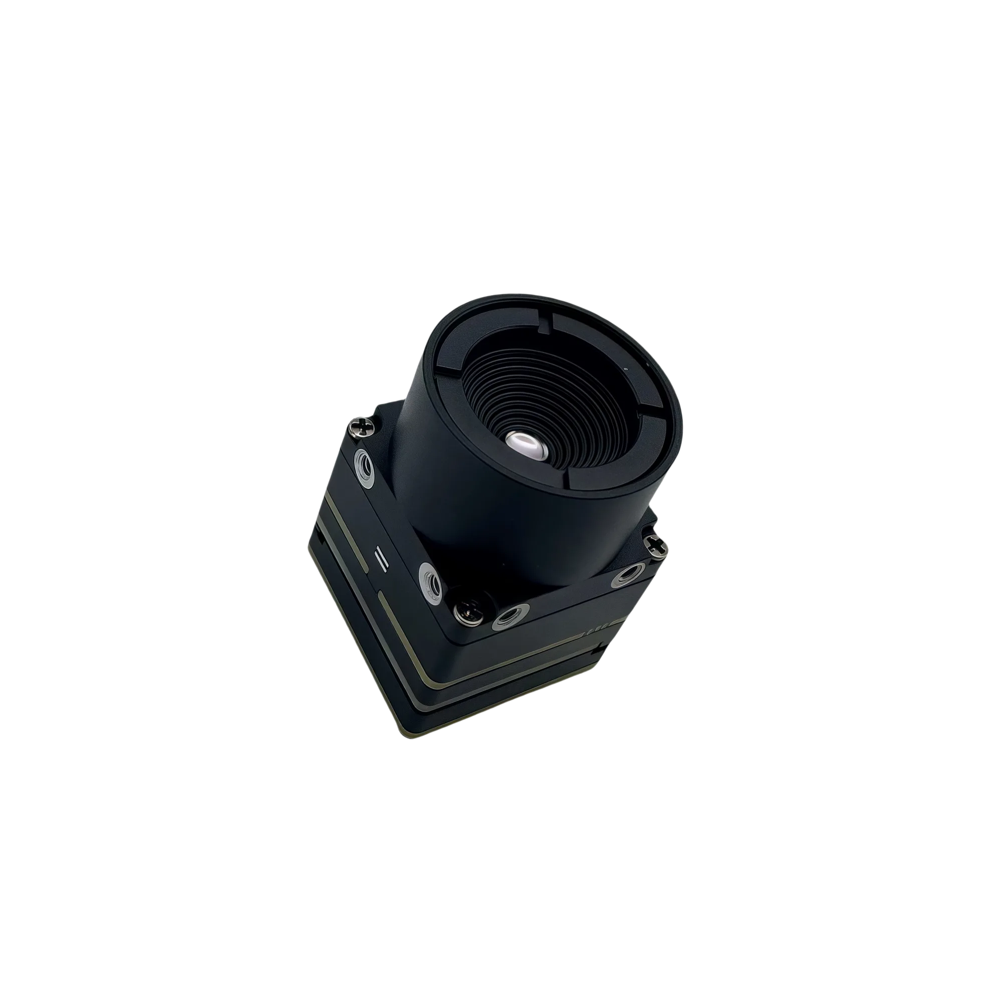
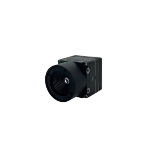
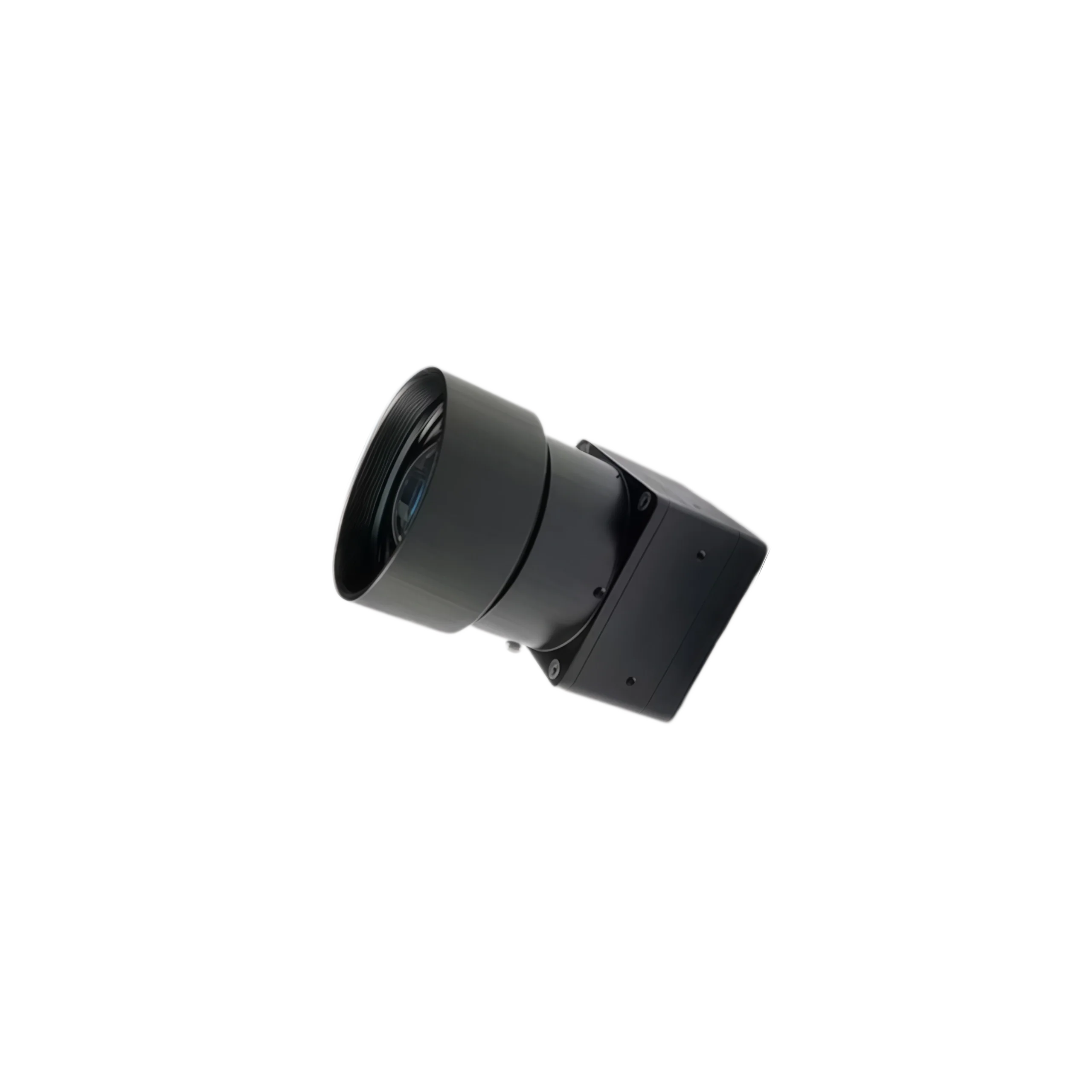
The NLIR1280L uncooled infrared core module represents the premier performance tier in high-definition Thermal Camera Cores. Engineered specifically for precision telemetry within drone gimbals, autonomous ADAS platforms, and industrial sensors, this module delivers mission-critical 1280×1024 infrared imaging with uncompromised structural efficiency.
- SWaP Advantage: 24.5g Ultralight Mass | 29mm × 29mm × 18.9mm Micro Framework optimized for space-constrained payloads.
- Environmental Resilience: Athermalized Optics ensure diffraction-limited clarity across extreme temperature fluctuations.
- High-Speed Dynamics: Native 30Hz frame rate guarantees fluid, real-time tracking telemetry.
1. Product Description | Thermal Camera Cores for UAV Payloads
As the industry’s most compact high-definition imaging engine, the NLIR1280L represents the pinnacle of uncooled Thermal Camera Cores. Engineered explicitly for size-constrained integration in UAV payloads (drones) and autonomous ADAS applications, this module is powered by a state-of-the-art 12μm pixel pitch longwave infrared (LWIR) detector, delivering a native 1280×1024 HD array for unparalleled thermal clarity.
Beyond its unmatched SWaP (Size, Weight, and Power) footprint, the NLIR1280L architecture is built for universal compatibility. It provides hardware integrators with versatile serial communication protocols and multiple digital video output interfaces, pairing seamlessly with our curated selection of lightweight athermalized infrared lenses. Whether deployed in rugged electro-optical tracking pods, low-visibility vision enhancement systems, automated machine vision setups, or rigorous scientific research, the NLIR1280L serves as the ultimate thermal sensor for demanding, mission-critical environments.
Strategic Target Application Domains
- Drones & UAVs: Acts as the primary telemetry payload for drone gimbals and heavy-lift industrial aerial systems.
- Automotive ADAS: Provides high-definition infrared vision enhancement for next-generation advanced driver assistance systems.
- Electro-Optical Pods: Integrates seamlessly into multi-sensor gyrostabilized gimbals and tracking pods.
- Vision Enhancement & Machine Vision: Delivers high-precision thermal analytics for automated manufacturing inspection and vision enhancement.
- Scientific Research: Provides raw, uncompressed thermal metadata essential for laboratory imaging and scientific research.
2. Lens Selection Matrix for Thermal Camera Cores
Table 2.1 Lens Parameters
| Array Format | Focal Length / F# | Lens Type | FOV (H×V) | IFOV |
|---|---|---|---|---|
| 1280×1024 | 10mm F1.2 | Athermalized | 78°×64.9° | 1.200 mrad |
| 1280×1024 | 35mm F1.0 | Athermalized | 25.1°×20.1° | 0.7 mrad |
| 1280×1024 | 50mm F1.2 | Athermalized | 17.4°×14° | 0.240 mrad |
| 1280×1024 | 75mm F1.2 | Athermalized | 11.67°×9.35° | 0.160 mrad |
3. Product Performance Parameters of LWIR Thermal Camera Cores
Table 3.1 Product Performance Parameters
| Item | Imaging Version | Temperature Measurement Version |
|---|---|---|
| Detector Type | VOx uncooled infrared FPA | VOx uncooled infrared FPA |
| Resolution | 1280×1024 | 1280×1024 |
| Pixel Pitch | 12μm | 12μm |
| Frame Rate | 30Hz | 30Hz |
| Spectral Band | 8–14μm | 8–14μm |
| NETD | ≤50mK @25℃, F/1.0 | ≤50mK @25℃, F/1.0 |
| Brightness/Contrast | Manual / Auto | Manual / Auto |
| Polarity | Black Hot / White Hot | Black Hot / White Hot |
| Pseudo Color | Supported(1) | Supported(1) |
| Image Processing | TECless NUC, Digital Filter, DDE | TECless NUC, Digital Filter, DDE |
| Image Mirror | Vertical / Horizontal / Diagonal | Vertical / Horizontal / Diagonal |
| Power Supply | 4.0–5.5VDC / 3.3V / 1.8V(2) | 4.0–5.5VDC / 3.3V / 1.8V(2) |
| Typical Voltage | 5VDC / 3.3V / 1.8V(2) | 5VDC / 3.3V / 1.8V(2) |
| Typical Power | 1.1W (0.9W)(3) | 1.2W (1.0W) (3) |
| Digital Video | 14/8bit LVCMOS, BT.1120, MIPI(4), USB3.0 | 14/8bit LVCMOS, CDS2, MIPI(4), USB3.0 |
| Control Interface | UART (3.3V) | UART (3.3V) |
| Temp Range | — | -20℃~+150℃; +100℃~+650℃ |
| Temp Accuracy | — | ±2℃ or ±2% of reading (whichever is greater) @Ambient temperature 15~35℃ |
| Temp Tools | — | Spot, line, area analysis |
| Weight | 24.5g | 24.5g |
| Dimensions | 29mm×29mm×18.9mm | 29mm×29mm×18.9mm |
| Operating Temp | -40℃~+70℃ | -40℃~+60℃ |
| Storage Temp | -45℃~+80℃ | -45℃~+80℃ |
| Humidity | 5–95%, noncondensing | 5–95%, noncondensing |
| Vibration | 6.06g random, 3axis 6directions | 6.06g random, 3axis 6directions |
| Shock | 80g, 4ms, halfsine, 3axis 6directions | 80g, 4ms, halfsine, 3axis 6directions |
Notes:
(1) Pseudo color not available for LVCMOS.
(2) Power consumption varies with input voltage.
(3) Power tested at 25℃, excluding interface board.
(4) LVCMOS / MIPI only available via Hirose 70pin; thermal module does not output temperature data via MIPI.
(5) Weight/dimensions exclude optics, housing, and extension board.
4. Hardware Interface Description for Thermal Camera Cores Connection
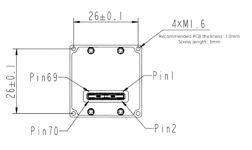
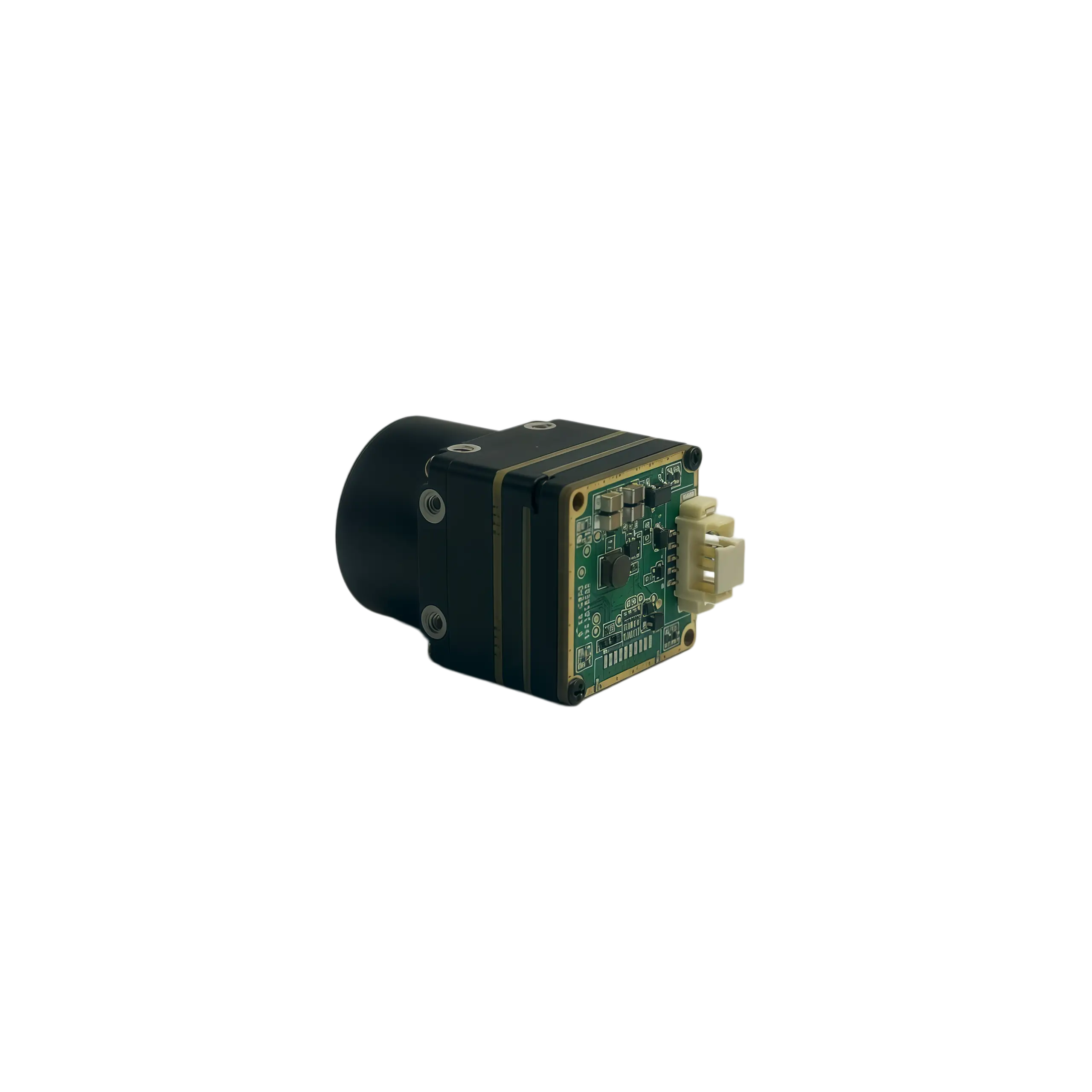
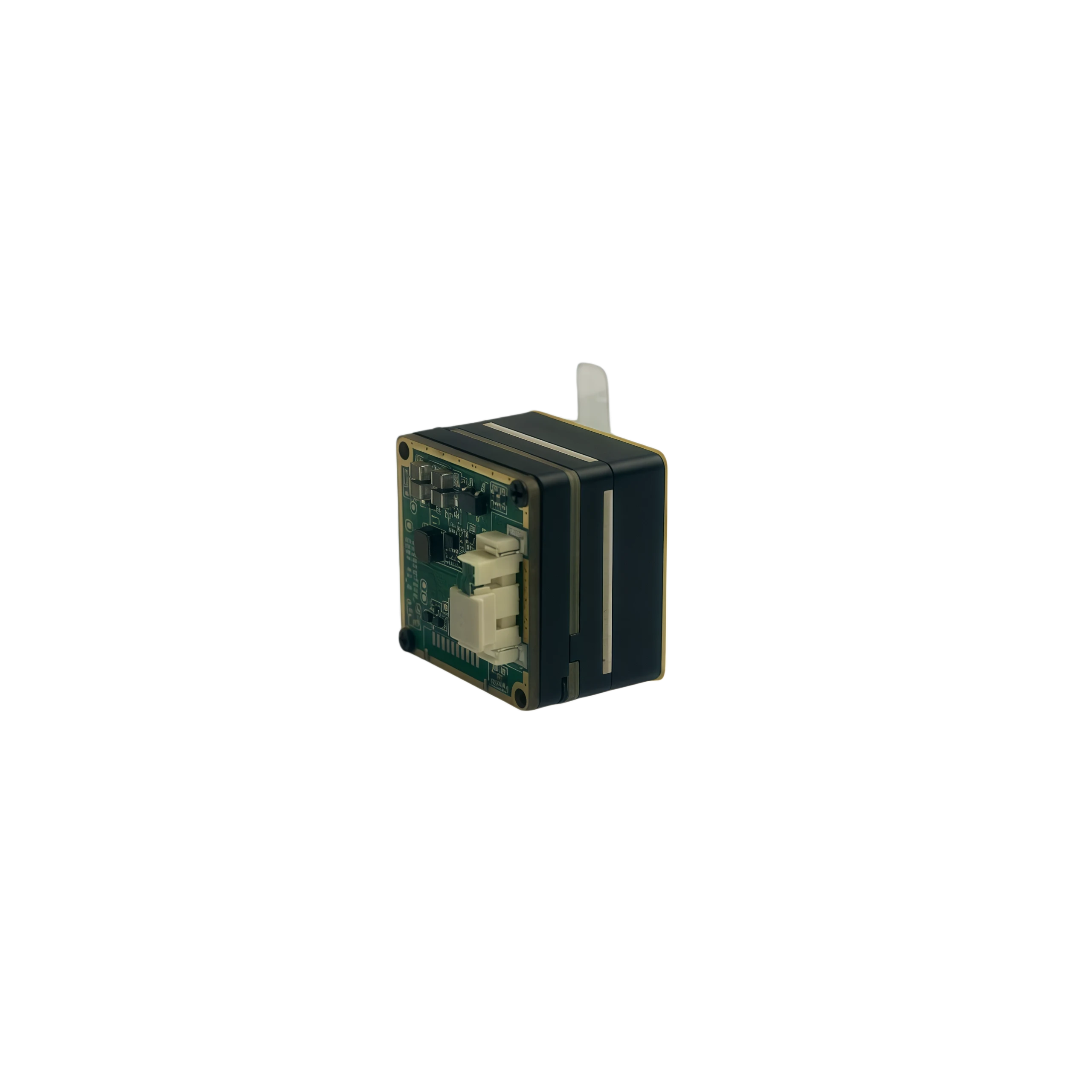
Figure 4.1 Core Assembly to User Interface
The module uses a Hirose 70pin DF40C-70DP-0.4V(51) connector, including power, UART, BT.1120, 8/14bit LVCMOS, 2lane MIPI, and 4 GPIOs.
4.1 Hirose 70pin Interface Definition
Table 4.1 Hirose 70pin User Interface Definition
| Pin No. | Name | Type | Description |
|---|---|---|---|
| 1–4 | Main Power | Power In | 4–5.5VDC(1) |
| 5,7 | 1.8V | Power In | Digital 1.8V |
| 6,8 | 3.3V | Power In | Digital 3.3V |
| 13 | UART_TX | Output | UART (3.3V)(2) |
| 14 | UART_RX | Input | |
| 30 | DV0 | Output | 14/8bit LVCMOS / BT.1120 / CDS2 (1.8V) Data signal LSB |
| 29 | DV1 | Output | Data signal |
| 32 | DV2 | Output | Data signal |
| 31 | DV3 | Output | Data signal |
| 34 | DV4 | Output | Data signal |
| 33 | DV5 | Output | Data signal |
| 36 | DV6 | Output | Data signal |
| 35 | DV7 | Output | Data signal MSB(8bit) |
| 38 | DV8 | Output | Data signal |
| 37 | DV9 | Output | Data signal |
| 40 | DV10 | Output | Data signal |
| 39 | DV11 | Output | Data signal |
| 42 | DV12 | Output | Data signal |
| 41 | DV13 | Output | Data signal MSB(14bit) |
| 44 | DV14 | Output | Data signal |
| 43 | DV15 | Output | Data signal MSB(16bit) |
| 46 | Frame_Valid | Output | Frame Valid Signal |
| 45 | Line_Valid | Output | Line Valid Signal |
| 47 | Clock_OUT | Output | Clock Signal |
| 48 | EXT_SYNC | Input | External sync (3.3V) |
| 15 | GPIO0 | I/O | GPIO (1.8V) |
| 17 | GPIO1 | I/O | |
| 58 | GPIO2 | I/O | |
| 60 | GPIO3 | I/O | |
| 57 | MIPI_DATA1+ | Output | 2lane MIPI |
| 59 | MIPI_DATA1- | Output | |
| 62 | MIPI_DATA2+ | Output | |
| 64 | MIPI_DATA2- | Output | |
| 61 | MIPI_ CLK+ | Output | |
| 63 | MIPI_ CLK- | Output | |
| 16,18,23,24,25,26,51,52,53,54,65,66,67,68 | – | – | N/C, Floating |
| 9–12,19–22,27–28,49–50,55–56,69–70 | GND | Power | Ground(3) |
Power Requirements:
Main Power: 4.0–5.5V, typical 5V, max 1A, ripple <40mVpp
1.8V: 1.75–1.85V, max 70mA
3.3V: 3.14–3.46V, max 50mA
 Figure 4.2 Core Power-On Timing Diagram
Table 4.2 Power Supply Requirements
| Pin | Voltage (Min. / Typ. / Max.) | Current (Min. / Typ. / Max.) | Maximum Ripple Noise |
|---|---|---|---|
| Main Power | 4.0V / 5V / 5.5V | —— / 200mA / 1A | 40mV |
| +1.8V | 1.75V / 1.8V / 1.85V | —— / 60mA / 70mA | 1mV (1Hz~50kHz) |
| +3.3V | 3.14V / 3.3V / 3.46V | —— / 20mA / 50mA | 50mV |
Note: TX and RX pins of the serial communication interface refer to the transmit and receive signals of the core module assembly respectively.
4.2 Digital Video Output Protocols for Advanced Integrations
Default output:
Imaging: BT.1120
Temperature measurement: CDS2
4.2.1 14bit or 8bit LVCMOS Digital Video
The core module assembly supports 14-bit or 8-bit LVCMOS digital video output. This digital video signal set consists of 1 clock signal (Clock), 1 line valid signal (Line_Valid), 1 frame valid signal (Frame_Valid), and 14 data signals (DV0 to DV13).
There are two pixel data bit depth options: When the user selects to output original (ORG) data or non-uniformity correction (NUC) processed data, the output bit depth is 14-bit, corresponding to data bus DV[13:0]. Among them, DV0 is the least significant bit (LSB), and DV13 is the most significant bit (MSB).
When the user selects to output dynamic range compression (DRC) processed image data, the output bit depth is 8-bit, corresponding to data bus DV[7:0]. Among them, DV0 is the least significant bit (LSB), and DV7 is the most significant bit (MSB). When 8-bit LVCMOS digital video output is enabled, the functions of brightness/contrast adjustment and polarity selection are supported. Pseudo-color conversion and image mirroring functions are not available.
Table 4.2 LVCMOS Clock Frequency
| Model No. | Clock Frequency |
|---|---|
| 1280 | 87.931MHz |
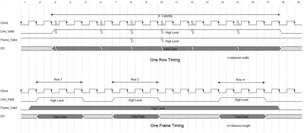 Figure 4.3 14-bit & 8-bit LVCMOS Digital Video Timing Diagram
Note:
(1) It is recommended to sample DV data on the rising edge of the Clock signal.
(2) Both Line_Valid and Frame_Valid signals are active high.
(3) After Line_Valid becomes active, it remains valid for n clock cycles. During this period, DV data is valid sequentially from the 1st column to the last column of the current row.
4.2.2 BT.1120 Timing Diagram
The core module assembly supports 16-bit BT.1120 digital video output. This digital video signal set consists of 1 clock signal (Clock), 1 line valid signal (Line_Valid), 1 frame valid signal (Frame_Valid), and 16 data signals (DV0 to DV15). The pixel data bit depth is 16-bit, with an image resolution of 1280×1024, and the image format is YUV422. The timing diagram is shown below.
Table 4.3 BT.1120 Clock Frequency
| Model No. | Clock Frequency |
|---|---|
| 1280 | 87.931MHz |
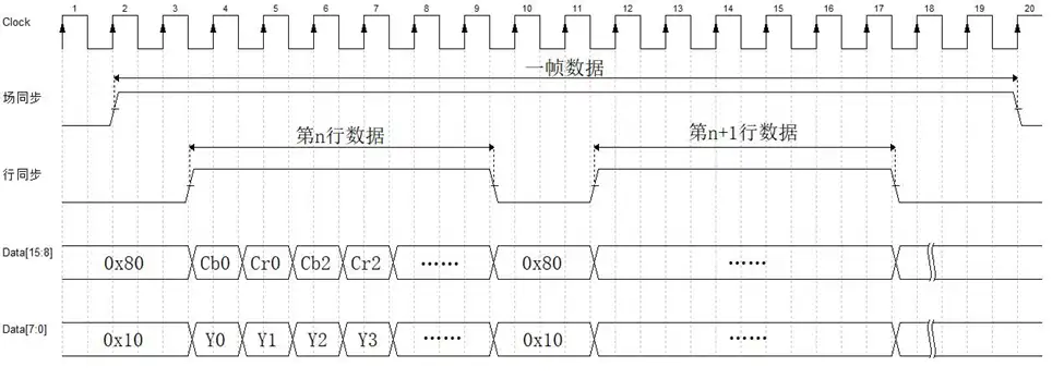 Figure 4.4 BT.1120 Digital Video External Synchronization Mode Timing Diagram
Table 4.4 BT.1120 Digital Video Internal Synchronization Mode Timing Structure
| Invalid Line EAV Code | Blanking Area | Invalid Line SAV Code | Invalid Data |
|---|---|---|---|
| 0xB6B6 | 0x8010 | 0xABAB | 0x8010 |
| Active Line EAV Code | Blanking Area | Active Line SAV Code | Active Data Area (CbYCrY) |
|---|---|---|---|
| 0x9D9D | 0x8010 | 0x8080 | Data area resolution of 1280 core module: 1280×1024 |
| Invalid Line EAV Code | Blanking Area | Invalid Line SAV Code | Invalid Data |
|---|---|---|---|
| 0xB6B6 | 0x8010 | 0xABAB | 0x8010 |
4.2.3 CDS2 Timing Diagram
The core module assembly supports 16-bit CDS2 digital video output. This digital video signal set consists of 1 clock signal (Clock), 1 line valid signal (Line_Valid), 1 frame valid signal (Frame_Valid), and 16 data signals (DV0 to DV15). The pixel data bit depth is 16-bit, with an overall image resolution of 2560×1024. The left 1280×1024 area adopts the YUV422 image format, while the right 1280×1024 area adopts the Raw16 temperature measurement data format. The timing diagram is shown below.
Table 4.5 CDS2 Clock Frequency
| Model No. | Clock Frequency |
|---|---|
| 1280 | 87.931MHz |
 Figure 4.5 CDS2 Digital Video Timing Diagram
Note: “Temp” represents temperature data. The valid data occupies the lower 14 bits, and the upper 2 bits are padded with 0.
4.2.4 MIPI Protocol
This product adopts 2-lane MIPI interface. The MIPI interface consists of 1 pair of source-synchronous differential clock signals (MIPI_CLK+, MIPI_CLK-), and 2 pairs of differential data signals (MIPI_DATA0+, MIPI_DATA0-, MIPI_DATA1+, MIPI_DATA1-).
The clock signal enters the High-Speed (HS) mode at the start of each frame, and exits High-Speed mode after each frame transmission is completed. During the inter-frame period, the interface operates in Low-Power (LP) mode (both data lines and clock line remain at 1.2V high level). The clock frequency of this product is 218MHz.
At the beginning of each frame, the data lanes transmit a Frame Start (FS) packet. At the end of each frame, a Frame End (FE) packet is transmitted. Between the Frame Start and Frame End packets, there are 1024 data long packets. Each long packet contains 1280×2 valid data words for one row of image, corresponding to 1280 pixels.
 Figure 4.6 Single Frame Data Structure Diagram
After power-on initialization, the core module assembly starts outputting MIPI digital video in RAW8 format (compliant with standard MIPI CSI-2 protocol).
The native output resolution is configured as (1280×2)×1024. The back-end device is required to reassemble the data into 1280×1024×16-bit data, with little-endian byte order (lower byte first).
Valid data per row is image pixel data. When pseudo-color function is enabled, the pixel arrangement follows the UYVY format (UV channel data precedes Y channel data), as illustrated in Figure 4.7.
 Figure 4.7 Schematic Diagram of One Line of Valid Data
4.3 User Extension Module Options
Table 4.6 User Extension Modules
| Model | Product Illustration | Main Interface | Compatible Cores |
|---|---|---|---|
| TLX04V100F016C | 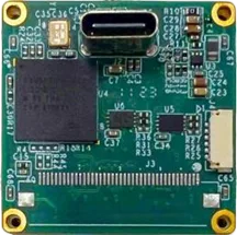 | USB3.0 TypeC, 5V | 1280 Imaging / 1280Temp |
5. Mechanical Dimensions and Mounting Blueprint
Module dimensions (without lens): 29mm × 29mm × 18.9mm
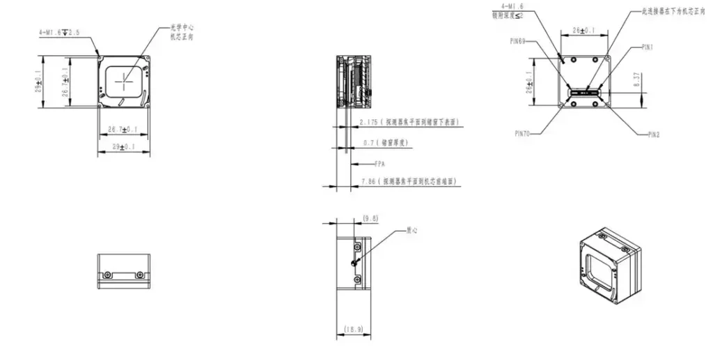 Mount: 4×M1.6
6. Precautions
- Do not point the module at intense radiation sources such as the sun.
- Recommended ambient temperature: -20℃ to 50℃.
- Do not touch or bump the detector window.
- Do not touch the device or cables with wet hands.
- Do not bend or damage cables.
- Do not clean with thinners.
- Disconnect power before plugging/unplugging cables.
- Avoid incorrect wiring.
- Observe ESD protection.
- Do not disassemble; contact us for service.
VIII. NTRON Precision Optoelectronic Technology & Systems


NLIR1280ES High-Performance Uncooled Thermal Camera Modules
VIEW SPECSRes.1280×1024Pitch12μmPWR≤ 5.0WDim./Wt.170±10gNLIR640 | 640×512 Uncooled Thermal Camera Module
VIEW SPECSRes.640×512Pitch12μmPWR< 0.7WDim./Wt.< 8.6gNLIR384 | 384×288 Balanced Industrial Thermal Module
VIEW SPECSRes.384x288Pitch12μmPWR< 0.42WDim./Wt.< 7g
NLIR640T Thermal Core <4g
VIEW SPECSRes.640×512Pitch8μmPWR≤ 0.4WDim./Wt.<4g (5)NLIR256 | Ultra-Low Power Infrared Thermal Module
VIEW SPECSRes.256×192Pitch12μmPWR< 0.35WDim./Wt.< 7g