0
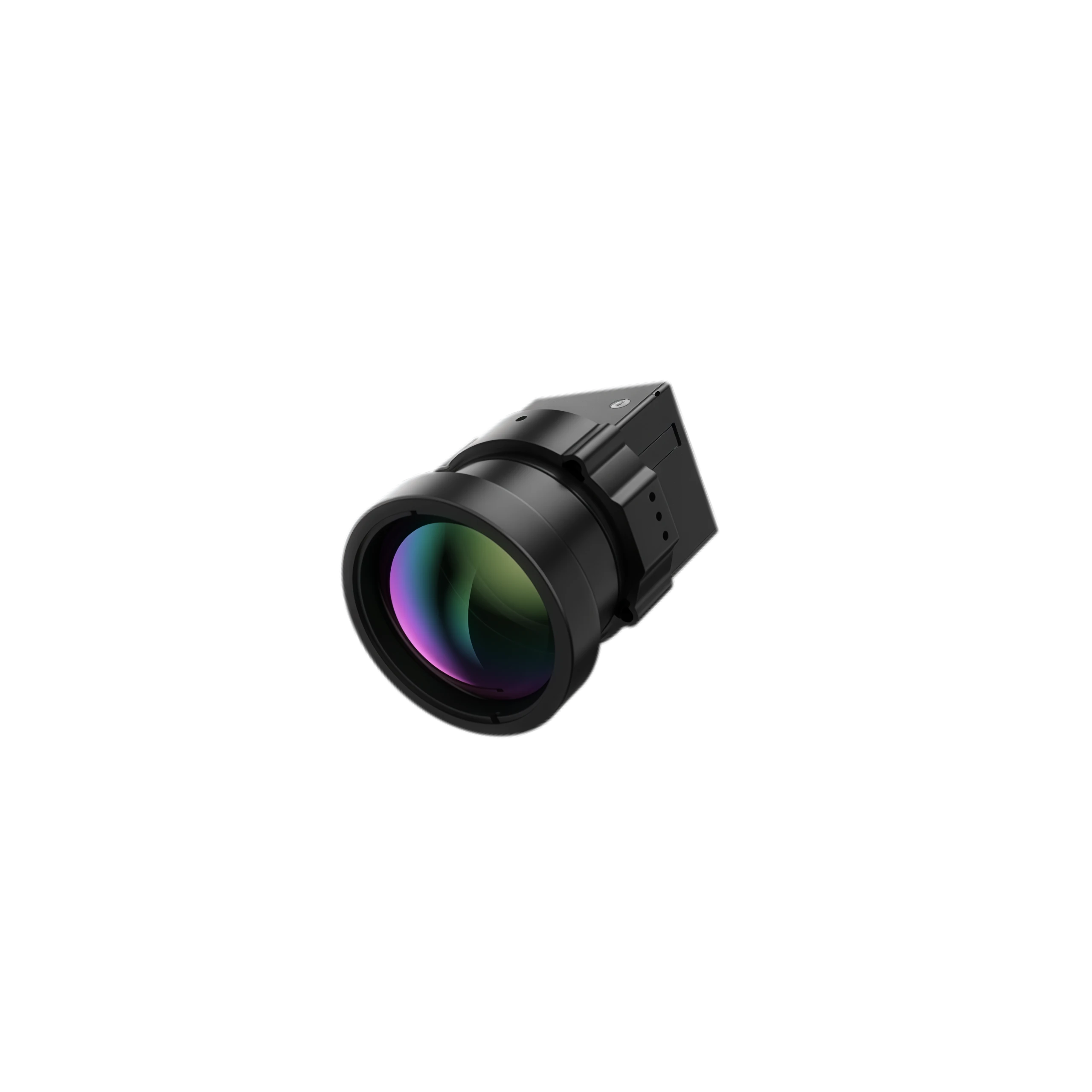
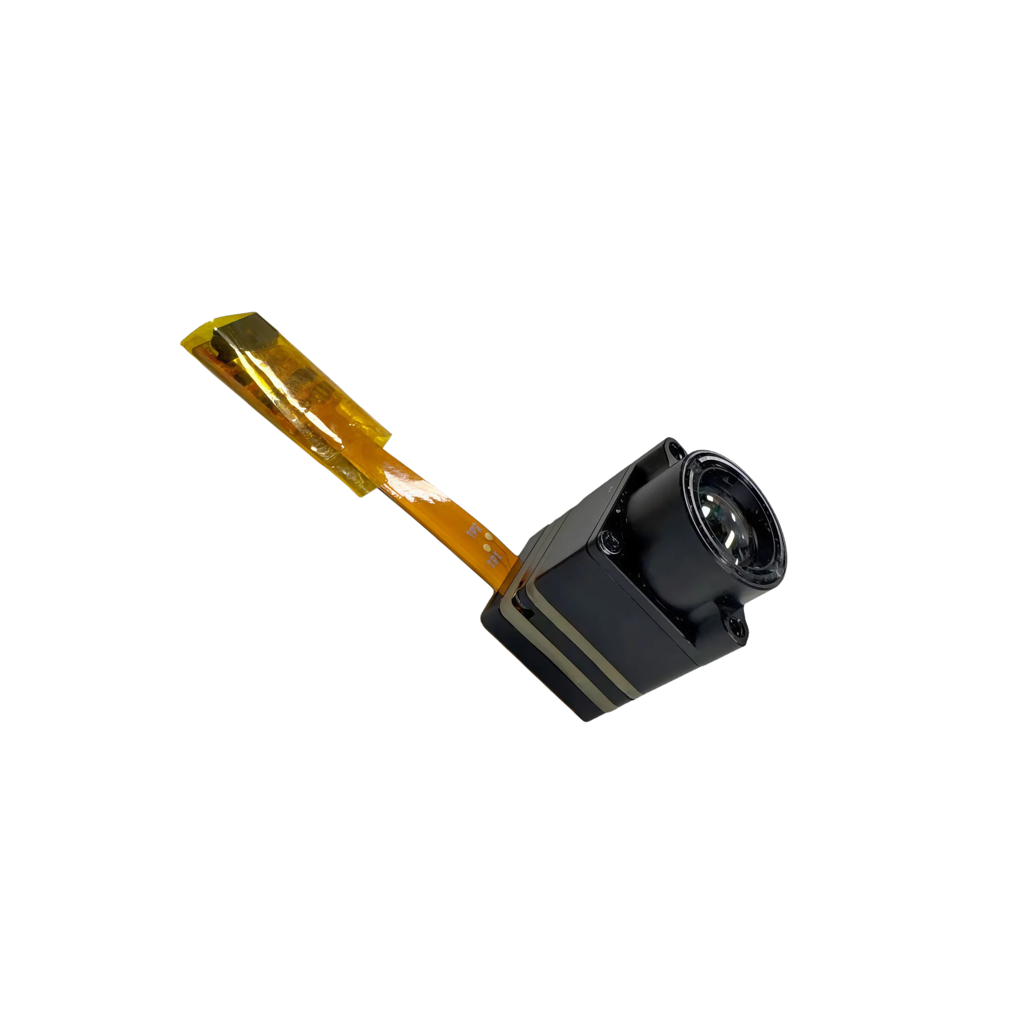
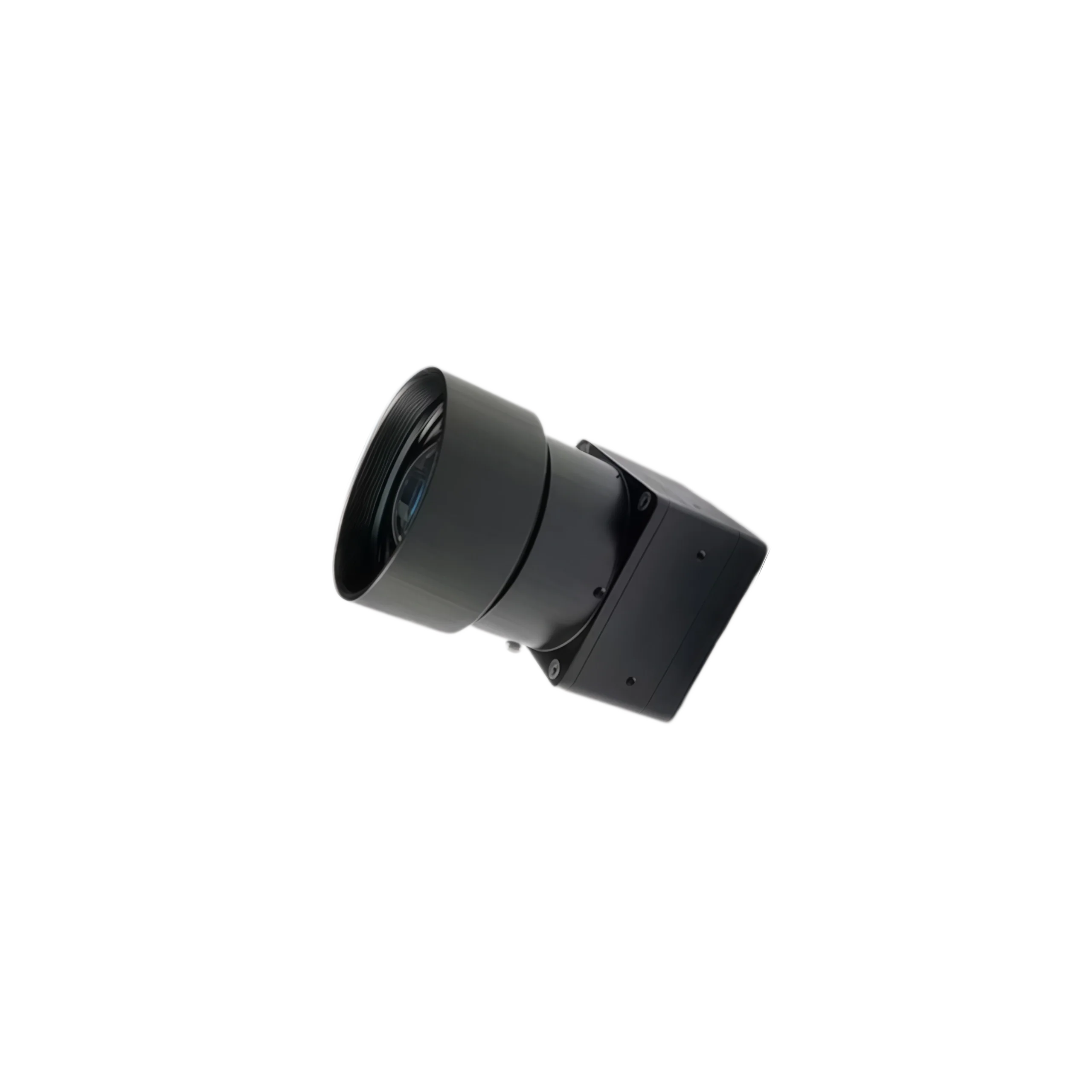
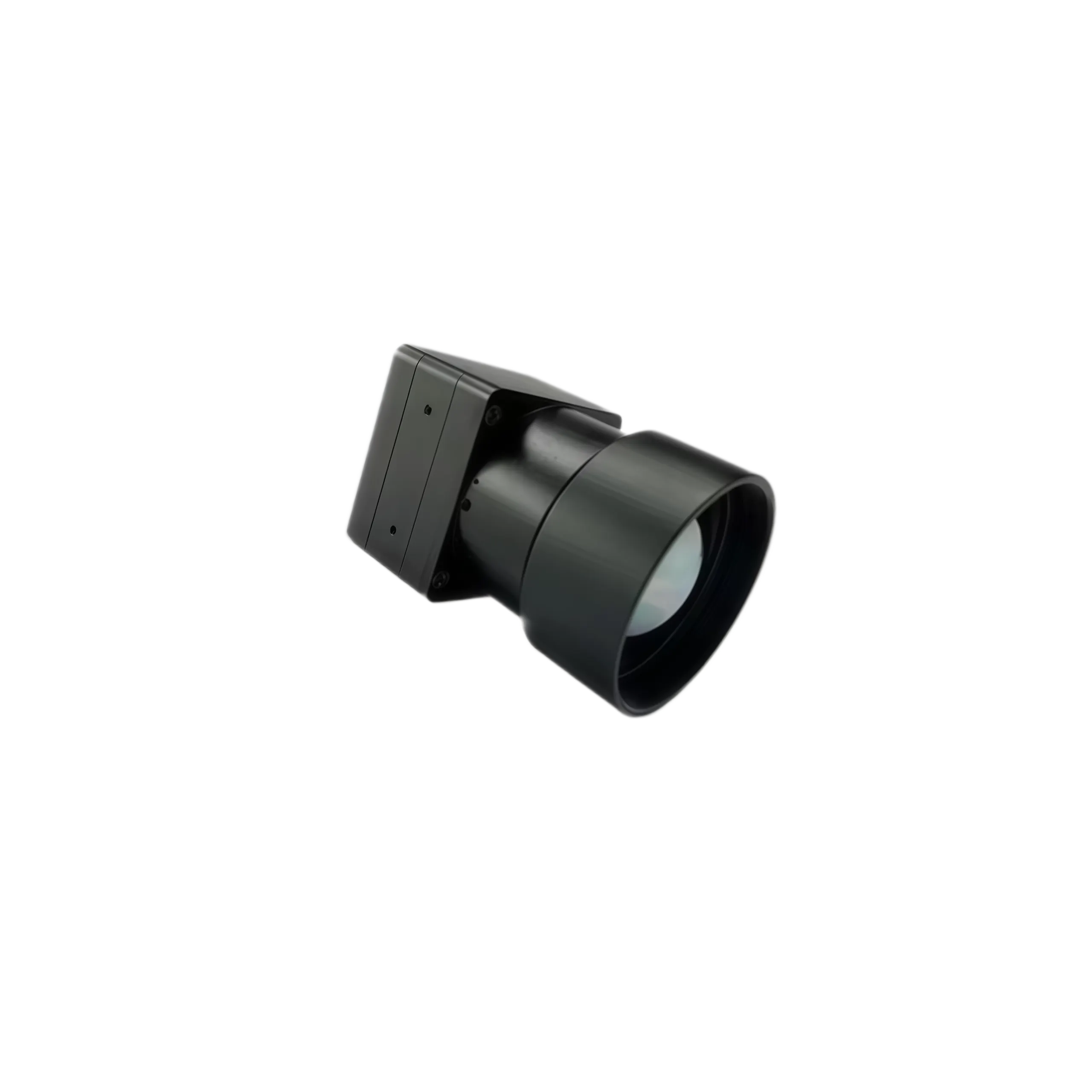
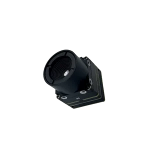
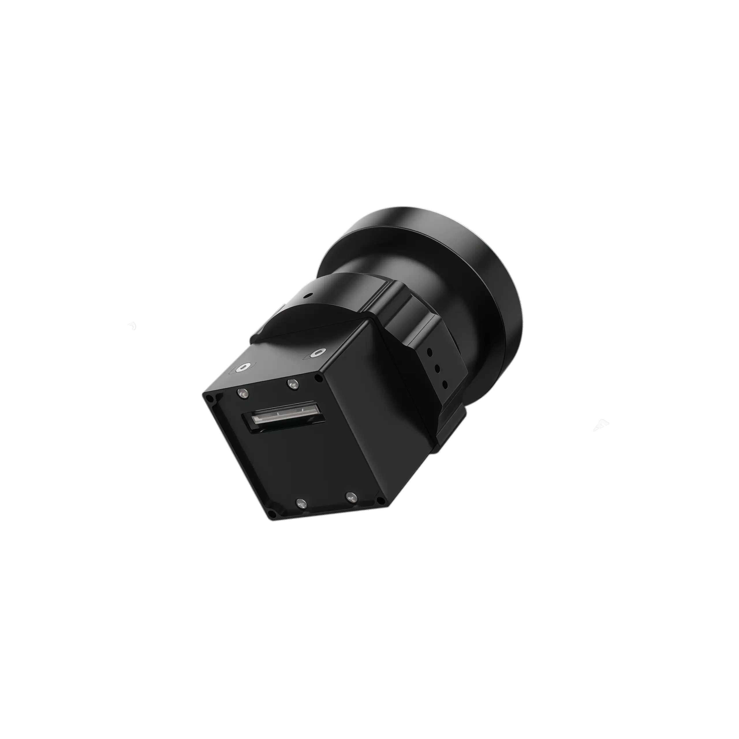
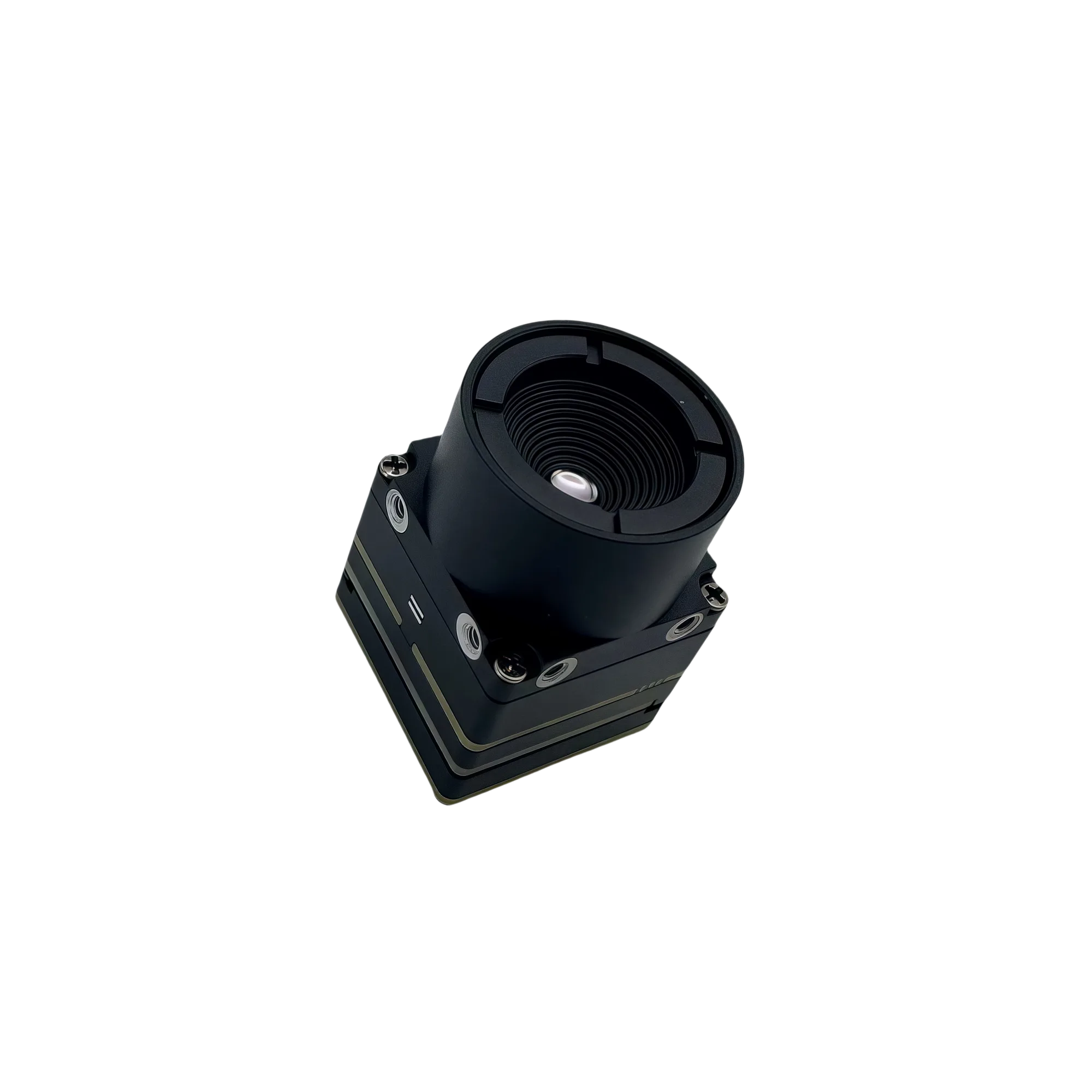
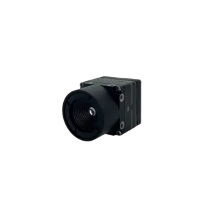
NLIR1280ES High-Performance Uncooled Thermal Camera Modules
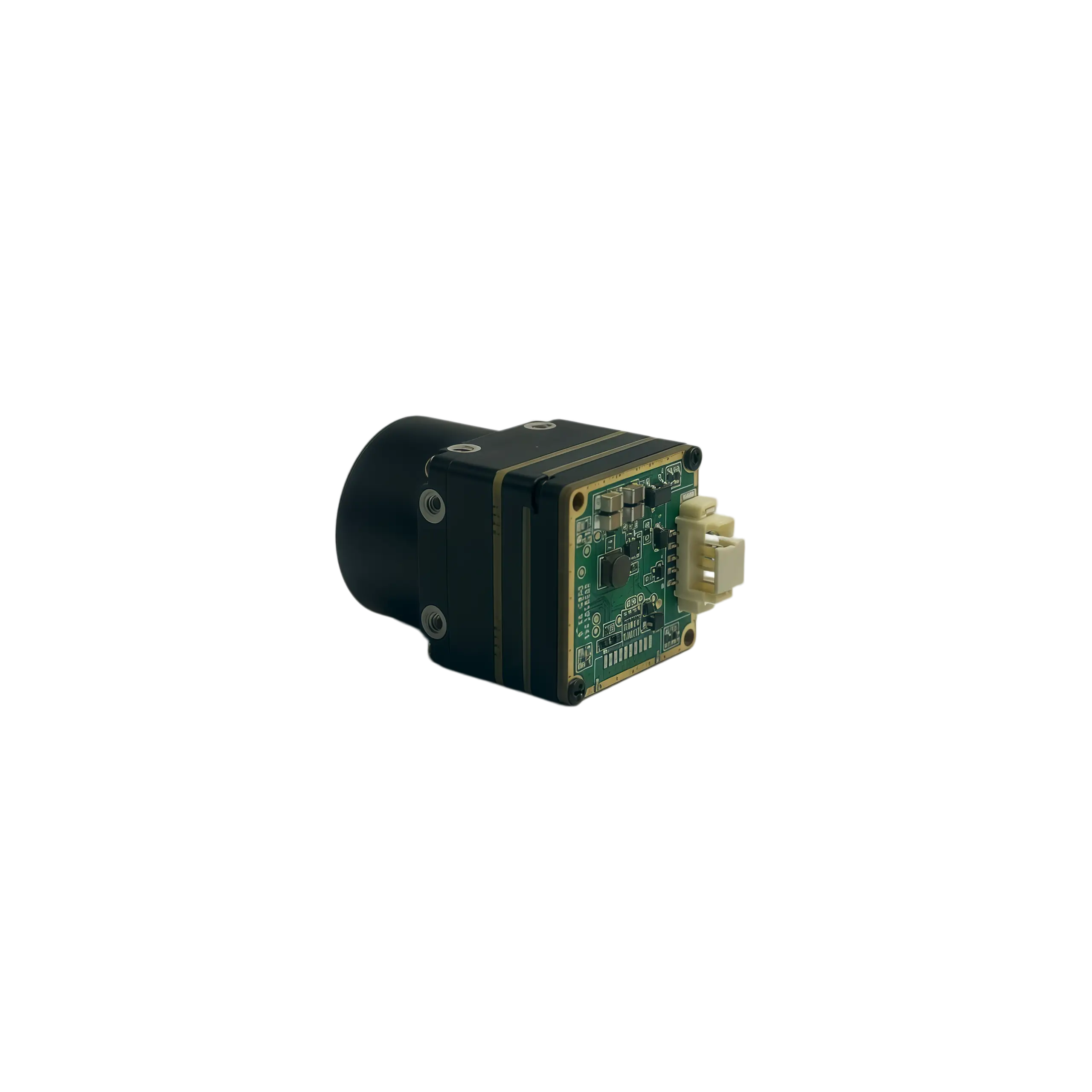
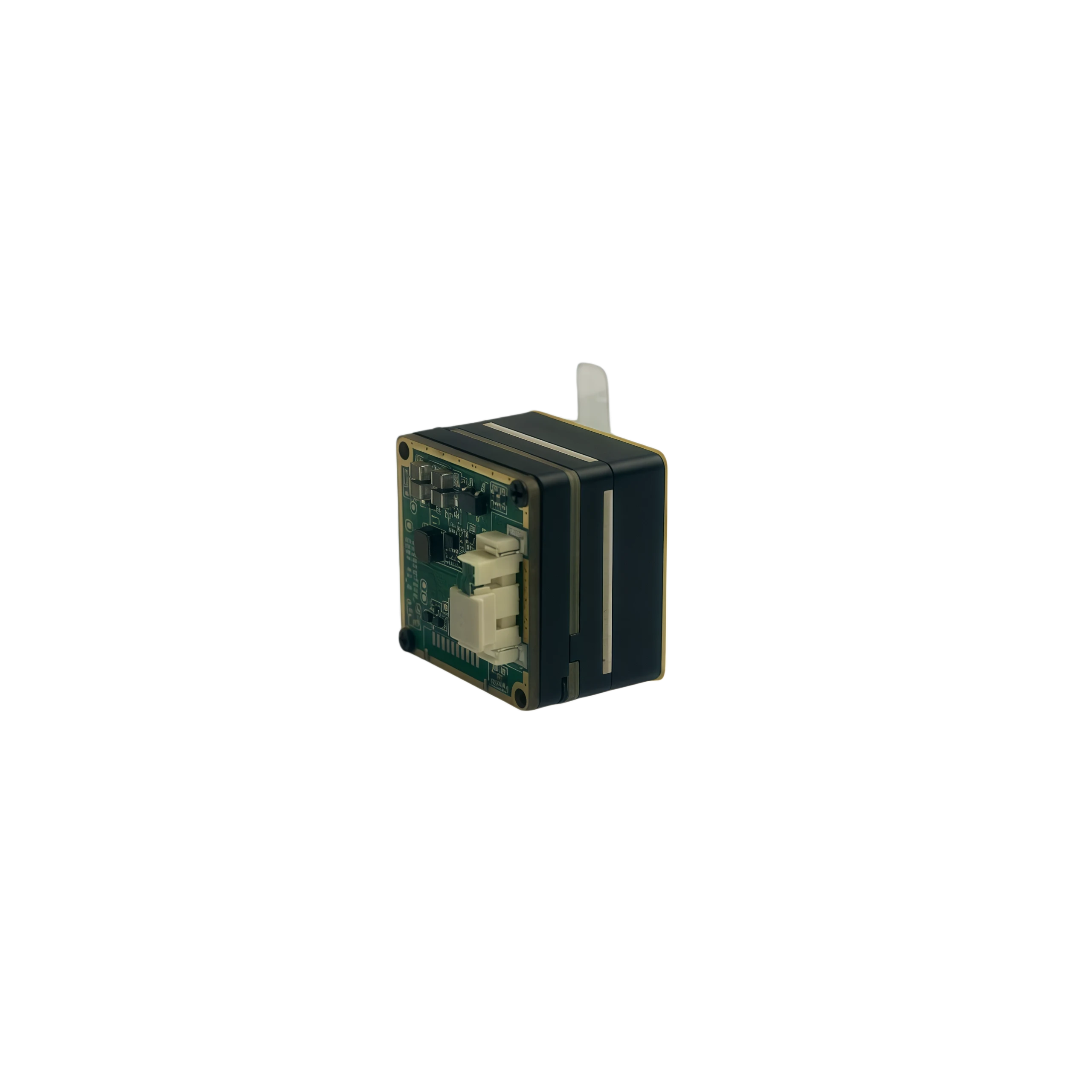
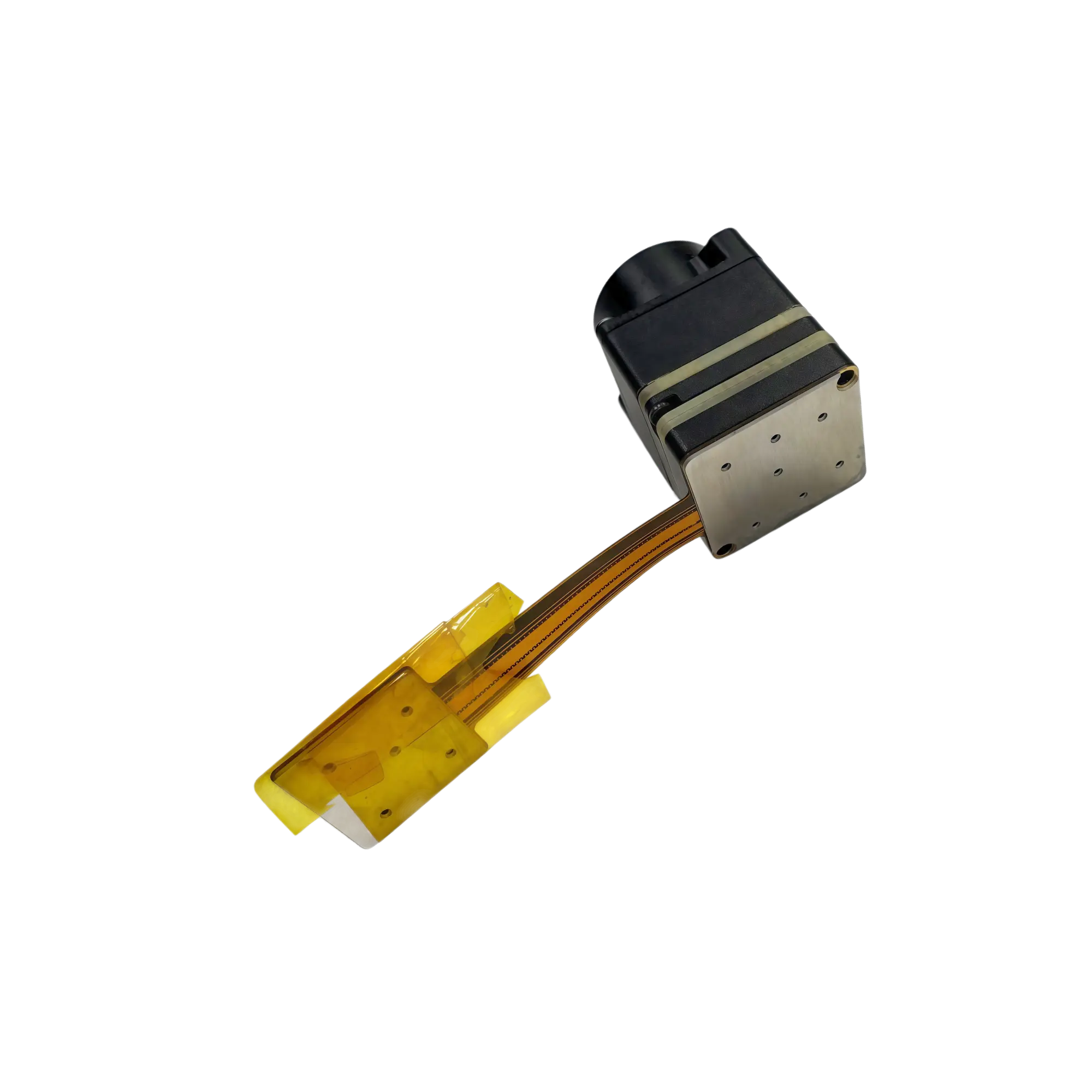
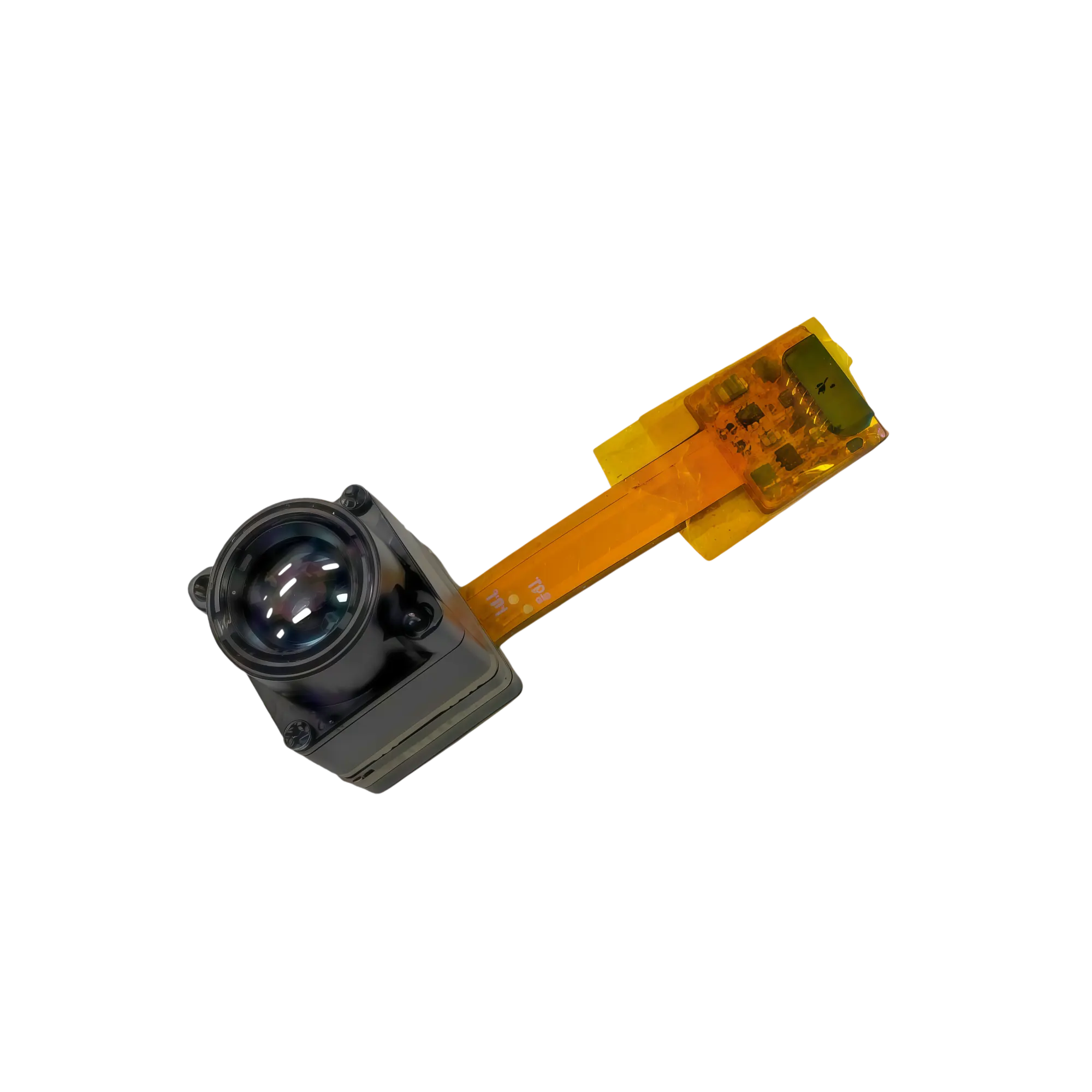
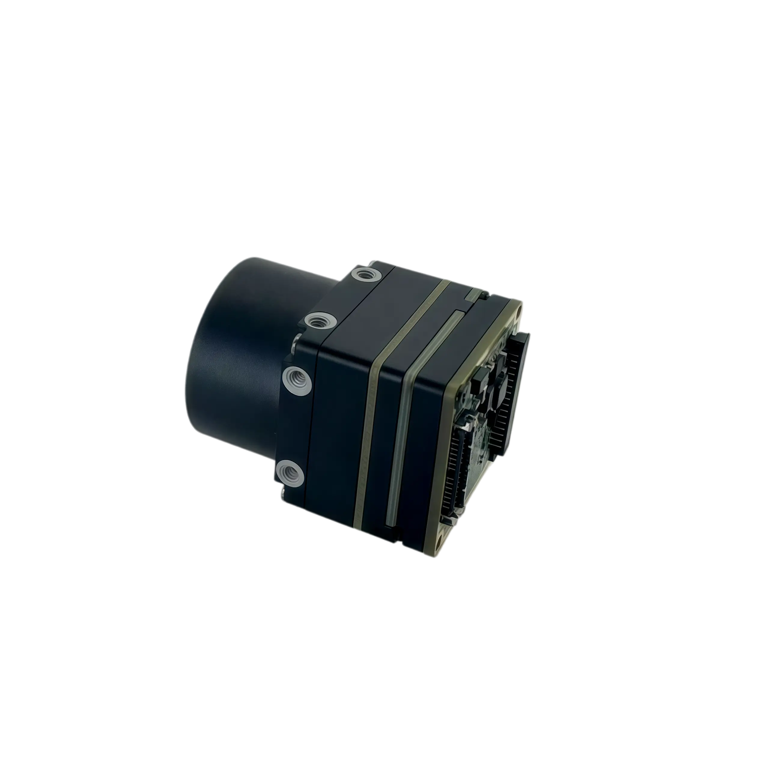
The NLIR1280ES uncooled infrared core module stands as the premier high-resolution network solution in modern Uncooled Thermal Camera Modules. Purpose-built for long-distance surveillance, perimeter security, and complex multi-node infrastructure networking, this system integrates advanced Ethernet capabilities with an ultra-sensitive 1280×1024 thermal framework to deliver unrivaled radiometric clarity.
- Network Architecture: Native Gigabit Ethernet TCP/IP output supporting ONVIF and GB28181 protocols for seamless IP camera streaming.
- Intelligent Analytics: Built-in hardware analytics including fire detection, tripwire, and region intrusion alarms.
- Superior Sensitivity: Features a ≤35mK NETD and high-speed 50Hz frame rate for capturing crisp telemetry in dynamic environments.
1. Product Description | High-Performance Uncooled Thermal Camera Modules
The 1280 uncooled thermal camera modules integrate a new-generation high-sensitivity vanadium oxide (VOx) infrared detector, delivering consistent high-performance core processing, ultimate imaging algorithms, and advanced lens control technology optimized for long-distance surveillance. Upgraded with next-generation imaging algorithms and paired with a 1280×1024 large-format sensor, this thermal imaging core is heavily optimized for challenging environmental conditions such as forests, sea surfaces, skies, rain, and fog, providing sharper and clearer infrared images.
To satisfy the demands of comprehensive infrastructure development, the module supports athermal fixed lenses, fixed-focus electric lenses, and continuous zoom lenses, enabling electric focusing, continuous zooming, auto-focusing, and defocus compensation. The architecture offers versatile video output interfaces including Ethernet, LVCMOS, BT.1120, and MIPI, with extensible hardware interfaces such as SDI, USB, CameraLink, and HDMI. An easy-to-use SDK is provided to shorten R&D cycles, improve efficiency, and reduce secondary development costs for integrators.
Strategic Target Application Domains
As one of the most reliable uncooled thermal camera modules available, the NLIR1280ES is widely deployed across demanding sectors requiring persistent observation:
- Perimeter Security: Establishes tight virtual fences and intelligent thermal tripwires.
- High-Altitude Observation: Mounted on elevated platforms for macro thermal analytics.
- Forest Fire Prevention: Continuously scans forestry to detect early-stage fire signatures.
- Water Area Monitoring: Pierces through maritime environments for vessel tracking.
- Industrial Temperature Measurement & Railway Monitoring: Provides non-contact thermal tracking for critical infrastructure and transit lines.
2. Athermal Lens Selection Matrix
Table 2.1 Athermal Lens
| Array Format | Focal Length / F# | Lens Type | FOV (H × V) | IFOV |
|---|---|---|---|---|
| 1280×1024 | 19mm F1.0 | Athermal | 46.53°×37.14° | 0.632mrad |
3. Product Performance Parameters of Networked Uncooled Thermal Camera Modules
Table 3.1 Performance Parameters
| Category / Item | Specification |
|---|---|
| General – Thermal Imager Model | 1280 Network Version |
| Detector Type | Vanadium Oxide Uncooled Infrared Focal Plane Array |
| Pixel Pitch | 12μm |
| Resolution | 1280×1024 |
| Frame Rate | 50Hz |
| Spectral Band | 8–14μm |
| NETD | ≤35mK @25℃, F#1.0 |
| Image Adjustment – Polarity | Black Hot / White Hot |
| Pseudo Color | 18 types supported |
| Electronic Zoom | 1.0–8.0× continuous (step 0.1), ROI zoom |
| Image Processing | Non-uniformity Correction (NUC) Temporal Filtering Spatial Filtering Brightness & Contrast Adjustment Digital Detail Enhancement (DDE) |
| Image Mirror | Horizontal / Vertical / Diagonal |
| Network Functions – Network Protocols | TCP/IP, UDP, ICMP, HTTP, HTTPS, FTP, DHCP, DNS, RTP, RTSP, RTCP, IGMP, SMTP, NTP, QoS |
| Platform Access | ONVIF, GB28181, SDK |
| Concurrent Preview Streams | Max. 20 channels |
| User Management | Max. 20 users, 3 levels: Admin, Operator, Guest |
| Browser | IE8+, Chrome, multi-language support |
| Intelligent Functions – Fire Detection | Supported |
| Intelligent Recording | Supported |
| Intelligent Alarm | Cable disconnection, IP conflict, storage full/error, unauthorized access detection & alarm |
| Intelligent Detection | Tripwire, region intrusion |
| Alarm Linkage | Recording / Snapshot / Email / PTZ / Alarm output |
| Lens Control – Lens Type | Fixed-focus electric / Continuous zoom |
| Auto Focus | Supported (focus time ≤1s near clear point) |
| Electric Focus / Zoom | Supported |
| Power – Typical Input Voltage | 12V DC ±10% |
| Typical Power Consumption @25℃ | ≤5.0W |
| Interfaces – Serial Comm. | 1×RS-485, 1×UART (PTZ control) |
| Ethernet | 10/100/1000M adaptive |
| Output | 1×MIPI (extensible MIPI input) |
| Audio / Alarm | 1×audio input, 1×audio output / 1×DV5V alarm input, 1×switch alarm output |
| Physical – Weight / Dimensions | 170±10g (without lens) / 45mm × 45mm × 50mm |
| Environment – Temp & Humidity | Op: -40℃ to +70℃ / Storage: -45℃ to +85℃ / 5–95% non-condensing |
| Environmental Certification | RoHS2.0 Compliant |
4. User Extension Component Selection for Uncooled Thermal Camera Modules
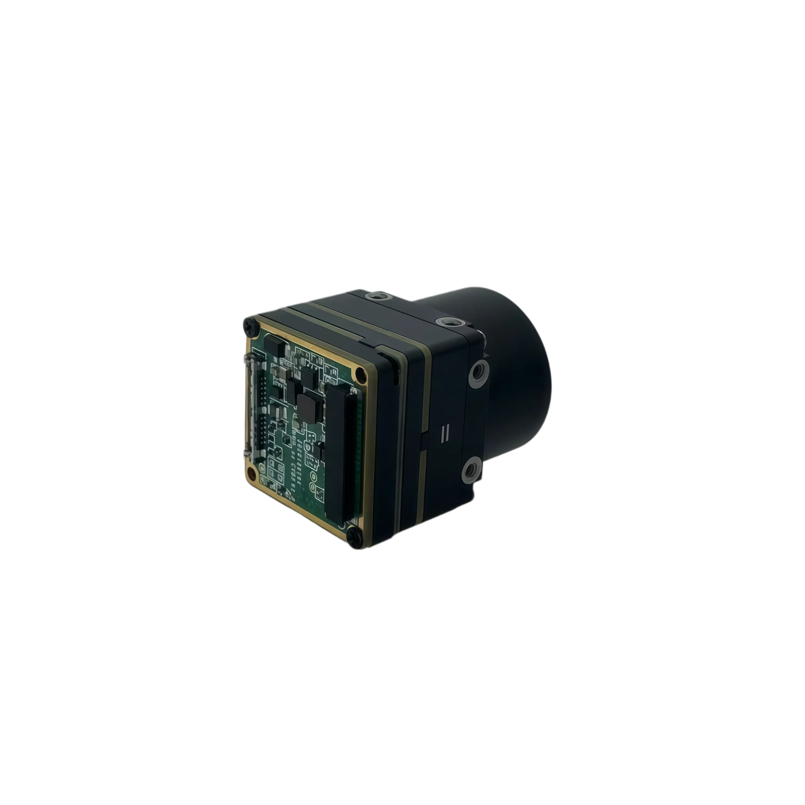
The user extension component is designed for the 1280 uncooled infrared core module. It contains 5 sockets as shown in Figure 4.1, supporting power input, RS-485, Ethernet, alarm I/O, audio I/O, MIPI and other interfaces. Interface definitions are shown in the figures below.
Table 4.1 User Extension Components
| Model | Product Diagram (Schematic) | Main Interfaces | Compatible Core |
|---|---|---|---|
| Network Board | 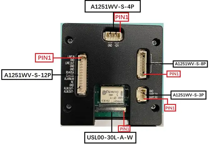 | • 12V DC power • RS-485 (Pelco only) • Ethernet • MIPI output • Lens motor interface • Audio I/O • Alarm I/O | 1280 |
4.1 User Extension Component Pin Definition
Figure 4.1 Extension Component | Contains 5 sockets supporting power, RS-485, Ethernet, alarm I/O, audio I/O, and MIPI.4.1.1 MIPI Socket
Table 4.2 USL00-30L-A-W 30-pin connector, providing MIPI output.
| Pin No. | Pin Name | Type | Description |
|---|---|---|---|
| 1–8 | NC | / | / |
| 9–12 | GND | Power | Ground |
| 13–17 | DC_IN | Power | DC input: 9V–12V |
| 18 | UART1_RX | Input | TTL 3.3V, core UART receive |
| 19 | UART1_TX | Output | TTL 3.3V, core UART transmit |
| 20 | GND | Signal GND | Signal ground |
| 21 | TXOUT0− | Signal | MIPI differential signal |
| 22 | TXOUT0+ | Signal | MIPI differential signal |
| 23 | TXOUT1− | Signal | MIPI differential signal |
| 24 | TXOUT1+ | Signal | MIPI differential signal |
| 25 | TXOUT2− | Signal | MIPI differential signal |
| 26 | TXOUT2+ | Signal | MIPI differential signal |
| 27 | TXOUTCLK− | Signal | MIPI differential signal |
| 28 | TXOUTCLK+ | Signal | MIPI differential signal |
| 29 | TXOUT3− | Signal | MIPI differential signal |
| 30 | TXOUT3+ | Signal | MIPI differential signal |
4.1.2 Power Socket
Table 4.3 A1251WV-S-4P 4-pin connector, for 12V power input.
| Pin No. | Pin Name | Type | Description |
|---|---|---|---|
| 1 | DC12V | Power | 12V DC input |
| 2 | DC12V | Power | 12V DC input |
| 3 | GND | Power | Ground |
| 4 | GND | Power | Ground |
4.1.3 Ethernet Socket
Table 4.4 A1251WV-S-8P 8-pin connector, supporting Gigabit Ethernet.
| Pin No. | Pin Name | Type | Description |
|---|---|---|---|
| 1 | ETH_DA+_1 | Input | Gigabit Ethernet differential Input |
| 2 | ETH_DA−_2 | Output | Gigabit Ethernet differential Output |
| 3 | ETH_DB+_3 | Input | Gigabit Ethernet differential Input |
| 4 | ETH_DC+_4 | Input | Gigabit Ethernet differential Input |
| 5 | ETH_DC−_5 | Output | Gigabit Ethernet differential Output |
| 6 | ETH_DB−_6 | Output | Gigabit Ethernet differential Output |
| 7 | ETH_DD+_7 | Input | Gigabit Ethernet differential Input |
| 8 | ETH_DD−_8 | Output | Gigabit Ethernet differential Output |
4.1.4 Function Socket
Table 4.5 A1251WV-S-12P 12-pin connector, providing audio I/O, alarm I/O and RS485.
| Pin No. | Pin Name | Type | Description |
|---|---|---|---|
| 1 | LINE_IN | Input | Audio input |
| 2 | GND | Signal GND | Audio input ground |
| 3 | LINE_OUT | Output | Audio output |
| 4 | GND | Signal GND | Audio output ground |
| 5 | GND | Signal GND | Signal ground |
| 6 | RS485A | I/O | RS485 I/O |
| 7 | RS485B | I/O | RS485 I/O |
| 8 | ALARM_IN | Input | Alarm input |
| 9 | NC | / | Not connected |
| 10 | GND | Signal GND | Alarm input ground |
| 11 | ALM_OUT+ | Output | Alarm output |
| 12 | ALM_OUT− | Output | Alarm output |
4.1.5 Serial Socket
Table 4.6 A1251WV-S-3P 3-pin connector for UART.
| Pin No. | Pin Name | Type | Description |
|---|---|---|---|
| 1 | UART_RX | Signal Output | UART signal input (+3.3V) |
| 2 | UART_TX | Signal Input | UART signal output (+3.3V) |
| 3 | GND | Power | Signal Ground |
4.1.6 Lens Control Socket
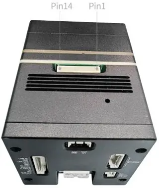 Figure 4.2 A1002WR-S-14P 14-pin connector for lens motor control.
Table 4.7 Screen Motor Control Connector Definition
| Pin No. | Pin Name | Type | Description |
|---|---|---|---|
| 1 | +3.3V | Power | 3.3V output |
| 2 | ZOOM_VOLTAGE | Input signal | Zoom potentiometer feedback |
| 3 | GND | Power | Ground |
| 4 | +3.3V | Power | 3.3V output |
| 5 | FOCUS_VOLTAGE | Input signal | Focus potentiometer feedback |
| 6 | GND | Power | Ground |
| 7 | +1.8V | Power | 1.8V output |
| 8 | TMP_SDA | I/O | Temperature sensor I2C SDA (1.8V) |
| 9 | TMP_SCL | Output | Temperature sensor I2C SCL (1.8V) |
| 10 | GND | Power | Ground |
| 11 | MOTOR_Z+ | I/O signal | Zoom motor + (12V) |
| 12 | MOTOR_Z− | I/O signal | Zoom motor − |
| 13 | MOTOR_F+ | I/O signal | Focus motor + (12V) |
| 14 | MOTOR_F− | I/O signal | Focus motor − |
4.2 Digital Video Format Description for Uncooled Thermal Camera Modules
4.2.1 LVCMOS Video Format
LVCMOS includes 1 clock, 1 frame sync (Fsync), 1 line sync (Lsync), and 14 parallel data signal lines. When a frame of data arrives, the frame synchronization signal is set to high level, indicating that the following data belong to the same frame. When the frame ends, the frame synchronization signal is set to low level, indicating the end of the frame. Similarly, when a line of data arrives, the line synchronization signal is set to high level; when the line ends, the line synchronization signal is set to low level.
The timing diagram of LVCMOS video is shown in the figure below.
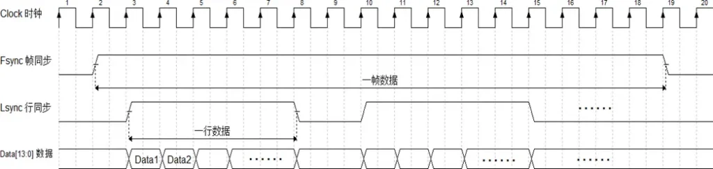 Figure 4.3 LVCMOS Video Timing Diagram
The LVCMOS video data source can be selected from original data (ORG), non-uniformity corrected data (NUC), image denoised data (DNS), and image processed data (DRC). Among these sources, DRC data is 8-bit per pixel, while all other sources are 14-bit per pixel. In the figure above, the synchronization signals and data signals change on the rising edge of the clock. In practical program design, signals can be set to change on the falling edge of the clock, so that the receiver can sample on the rising edge of the clock. Data sources: ORG, NUC, DNS (14-bit), DRC (8-bit).
Table 4.8 LVCMOS Clock Frequency
| Core Model | Clock Frequency |
|---|---|
| 1280 (50Hz) | 77 MHz |
4.2.2 BT.1120 Video Format
For the BT.1120 digital video timing of the uncooled infrared core module, there are two modes: internal synchronization and external synchronization. Internal synchronization uses synchronization reference codes to indicate the start and end of each line or frame. It includes 16 data lines and 1 clock line. External synchronization includes 16 data lines, 1 clock line, plus one line synchronization signal and one field synchronization signal.
The default BT.1120 digital video source is DRC and cannot be modified. The BT.1120 video output by the uncooled infrared core module supports both internal and external synchronization modes. That is, the 16 data lines carry synchronization reference codes, while line sync and field sync signals are also output simultaneously. Data transitions on the falling edge of the clock to ensure stable sampling at the receiving end on the rising edge of the clock. The video resolution output by the 1280 core is 1280 columns × 1024 lines.
4.2.2.1 External Sync Timing
At line sync, 16-bit data outputs: high 8-bit chroma, low 8-bit luma. During blanking: outputs 0x8010.
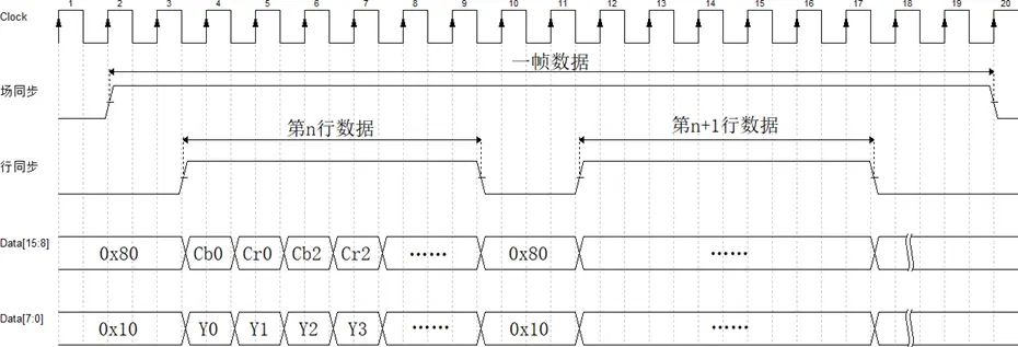 Figure 4.4 BT.1120 External Sync Output Timing Diagram
4.2.2.2 Internal Sync Timing
Table 4.9 BT.1120 Internal Sync Output Format Timing Diagram
| Row Type | EAV (End of Active Video) | Blanking Area | SAV (Start of Active Video) | Payload / Data Area |
|---|---|---|---|---|
| Inactive Row | Inactive Row Reference Code (EAV) | Blanking Area 0x8010 | Inactive Row Reference Code (SAV) | Blanking Area 0x8010 |
| Active Row | Active Row Reference Code (EAV) | Blanking Area 0x8010 | Active Row Reference Code (SAV) | Active Data Area (For the 1280 core, the data area size is 1280 × 1024) |
| Inactive Row | Inactive Row Reference Code (EAV) | Blanking Area 0x8010 | Inactive Row Reference Code (SAV) | Blanking Area 0x8010 |
The table above illustrates the format of a single frame of video. A frame consists of inactive rows and active rows, as well as blanking areas and active data areas. The top-left corner of the table corresponds to the start of the frame, and the bottom-right corner corresponds to the end of the frame. The specific frame size, the number of inactive/active rows, and the size of the blanking areas are determined by the actual configuration of the core module. All data in the blanking area is set to 0x8010. Each reference code occupies 4 clock cycles, and each pixel data occupies 1 clock cycle. Both the reference codes and pixel data are 16-bit. The format of the reference codes is shown in the table below:
Table 4.10 Reference Code Format
| EAV | SAV | |
|---|---|---|
| Invalid Line | 0xFFFF 0x0000 0x0000 0xB6B6 | 0xFFFF 0x0000 0x0000 0xABAB |
| Valid Line | 0xFFFF 0x0000 0x0000 0x9D9D | 0xFFFF 0x0000 0x0000 0x8080 |
In the internal synchronization mode, the 16-bit active pixel data is also structured as follows: the high 8 bits are chroma data, and the low 8 bits are luma (grayscale) data. Each reference code begins with three clock cycles of 0xFFFF, 0x0000, and 0x0000.
Table 4.11 BT.1120 Clock Frequency
| Core Model | Clock Frequency |
|---|---|
| 1280 (50Hz) | 77 MHz |
4.2.3 CDS_2 Video Format
The CDS_2 video of the 1280 core is based on BT.1120 video with additional temperature data, enabling simultaneous output of image data and temperature data. In CDS_2 video, the output image is identical to BT.1120 video; however, the bit order within each pixel is reversed: In CDS_2, the high 8 bits are luminance (Y), and the low 8 bits are chrominance (CbCr). This is the opposite of the standard BT.1120 format.
The overall structure of CDS_2 video is very similar to BT.1120, with the only difference being that temperature data is embedded within the active data payload. CDS_2 video requires the following signals: 1 clock line (clk), 1 frame sync line (fsync), 1 line sync line (lsync), 16 parallel data lines. The signals use a 3.3V high level and 0V low level. When outputting temperature data, the two most significant bits (MSBs) of the 16-bit data bus are driven low. The DVP-interface CDS_2 video format is only supported for 1280@30Hz core modules.
The data format of one frame of CDS_2 video is shown in the table below:
Table 4.12 CDS_2 Frame Data Format
| Row Type | EAV (End of Active Video) | Blanking Area | SAV (Start of Active Video) | Payload/Data Area |
|---|---|---|---|---|
| Inactive Row | Inactive Row Reference Code (EAV), 0xB6B6 | Blanking Area 0x8010 | Inactive Row Reference Code (SAV), 0xABAB | Invalid Data 0x8010 |
| Active Row | Active Row Reference Code (EAV), 0x9D9D | Blanking Area 0x8010 | Active Row Reference Code (SAV), 0x8080 | Active Data Area (Image Data), YCbYCr, 1280 × 1024 |
| Inactive Row | Inactive Row Reference Code (EAV), 0xB6B6 | Blanking Area 0x8010 | Inactive Row Reference Code (SAV), 0xABAB | Invalid Data 0x8010 |
The internal synchronization codes of CDS_2 video are identical to those of BT.1120 video. CDS_2 video also supports both internal and external synchronization modes. In addition to the clock and data signals, it includes line synchronization and frame synchronization signals. The high-level duration of the line sync signal in CDS_2 video is twice that of BT.1120 video. For the 16-bit image data, the high 8 bits represent luminance (Y), and the low 8 bits represent chrominance (CbCr). The timing format of a line containing active data in CDS_2 video is shown in the figure below:
 Figure 4.5 CDS_2 Video Timing Diagram
4.2.4 MIPI Interface
The MIPI video format serializes parallel digital video data using the MIPI protocol. Depending on the selected original parallel digital video format, the 1280 core can output image data independently. The MIPI video of the 1280 core adopts the CSI-2 interface standard with D-PHY physical layer and 4-lane transmission, requiring 1 pair of high-speed differential clock signal lines and 4 pairs of high-speed differential data signal lines.
MIPI-CSI uses standard short packets for synchronization. Each frame consists of the vertical blanking area, frame start packet (FS), frame end packet (FE), line blanking area, and data long packets. A data long packet includes a packet header (PH), packet footer (PF), and an active data area. A simplified diagram of one frame of MIPI video output by the core is shown in the table below:
Table 4.13 MIPI Frame Data Format
| Vertical Blanking (spanning the entire row) | |||||
| Vertical Blanking | FS (Frame Start) | Horizontal Blanking | Packet Header (PH) | Active Data Area | Packet Footer (PF) |
| Horizontal Blanking (spanning the entire row) | |||||
| Horizontal Blanking | FE (Frame End) | Vertical Blanking (spanning the rest of the row) | |||
| Vertical Blanking (spanning the entire row) | |||||
The frame synchronization short packets (FS/FE) of MIPI video include Data ID, Short Packet Data Field, and VCX + ECC. The header (PH) of a data long packet contains Data ID, Word Count, and VCX + ECC, while the footer (PF) is a checksum using the CCITT-standard CRC16 algorithm. Packets are connected via EOT-LPS-SOT. The frame synchronization short packet format is shown in Table 4.14 below, the packet header/footer format in Table 4.15, and the EOT and SOT formats in Table 4.16.
For the 1280 core, the default output data format is YUV422 8 ‑ bit, transmitted in UYVY order. The line timing is shown in Figure 4.6. The clock signal enters high ‑ speed mode at the start of each frame and exits high ‑ speed mode at the end of the frame. Between frames, the interface enters low ‑ power mode (both data and clock lines are held at 1.2V high level). The frame timing is shown in Figure 4.7:
Table 4.14 MIPI D-PHY Frame Start/End Short Packet Format
| 8-bit Data ID | 16-bit Short Packet Data Field | 8-bit VCX + ECC | |
|---|---|---|---|
| FS (Frame Start) | 0x00 | 1280 core default: 0x0000 | Generated by ECC calculation |
| FE (Frame End) | 0x01 |
Table 4.15 MIPI Packet Header/Footer Format
| 8-bit Data ID | 16-bit Word Count | 8-bit VCX + ECC | |
|---|---|---|---|
| PH (Packet Header) | 0x1E | {Word Count[7:0], Word Count[15:8]} | Generated by ECC calculation |
| PF (Packet Footer) | {CRC[7:0], CRC[15:8]} |
Table 4.16 EOT/SOT Format
| Entry | Description |
|---|---|
| 8-bit EOT | The last transmitted bit is inverted. |
| 8-bit SOT | 0xB8 |
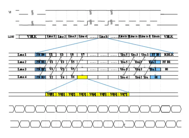
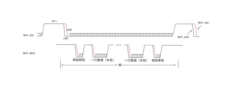 Figure 4.6 & 4.7 MIPI Video Line and Frame Timing Diagram
Table 4.17 MIPI Clock Frequency
| Core Model | Lane Rate | Clock Frequency |
|---|---|---|
| 1280 (50Hz) | 1360 Mbps | 680 MHz |
5. Product Drawings
Note: Dimensions of these uncooled thermal camera modules vary with different lenses and extension components.
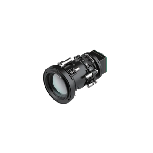 Figure 5.1 1280 Core – Lens 01 Series Core Drawing
6. Precautions
- To protect your uncooled thermal camera modules and others from injury and prevent equipment damage, please read all information before use.
- Do not direct the thermal imager at intense radiation sources such as the sun.
- Recommended operating temperature: -20℃ to 50℃.
- Do not touch or bump the detector window with hands or foreign objects.
- Do not touch the device or cables with wet hands.
- Do not bend or damage cables.
- Do not clean the device with diluents.
- Do not plug/unplug cables while powered on.
- Avoid incorrect wiring to prevent damage.
- Protect against static electricity.
- Do not disassemble the device; contact the manufacturer for professional repair in case of failure.
VIII. NTRON Precision Optoelectronic Technology & Systems


NLIR640 | 640×512 Uncooled Thermal Camera Module
VIEW SPECSRes.640×512Pitch12μmPWR< 0.7WDim./Wt.< 8.6g
NLIR640T Thermal Core <4g
VIEW SPECSRes.640×512Pitch8μmPWR≤ 0.4WDim./Wt.<4g (5)NLIR384 | 384×288 Balanced Industrial Thermal Module
VIEW SPECSRes.384x288Pitch12μmPWR< 0.42WDim./Wt.< 7gNLIR1280L | Thermal Camera Cores for UAV Payloads
VIEW SPECSRes.1280 × 1024Pitch12μmPWR~1.1WDim./Wt.24.5gNLIR256 | Ultra-Low Power Infrared Thermal Module
VIEW SPECSRes.256×192Pitch12μmPWR< 0.35WDim./Wt.< 7g